Timothy Kozono, Linear Technology
Design Note 560
Introduction
The LTC3623 is a high efficiency, monolithic synchronous step-down regulator capable of sourcing or sinking up to 5 A of continuous output current from an input voltage range of 4 V to 15 V. Its compact 3 mm × 5 mm QFN package incorporates an abundance of features including a low EMI Silent Switcher® architecture, output voltage cable drop compensation and single resistor output voltage programming. The constant frequency/controlled on-time architecture responds quickly to line and load transients even in low duty cycle, high frequency applications. The device offers a 400 kHz to 4 MHz operating frequency range with multiple optional protection and monitoring features, enabling compact, robust solutions. VIN regulation, discontinuous/continuous mode and a supply current less than 1 μA during shutdown make this regulator suitable for a wide range of power applications.
A single resistor is used to set the internal reference voltage for the part. The adjustable internal reference voltage sets the output voltage and allows the output voltage to operate rail-to-rail, from 0 V to VIN. The reference voltage can be driven directly as an audio driver or configured to operate as a TEC driver. Capable of sourcing or sinking 5 A of output current, the regulator moves the output voltage quickly in either direction. The output current monitor signal can be used to increase the reference voltage to compensate for output voltage drop caused by cable resistance.
3.3 V Output, 1 MHz Buck Regulator
 |
||
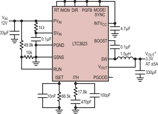
| Figure 1. | High Efficiency 12 V to 3.3 V 1 MHz Step-Down Regulator with Programmable Reference. |
|
 |
||
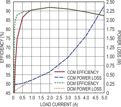
| Figure 2. | Efficiency and Power Loss for the Application in Figure 1 in CCM and DCM Mode. |
|
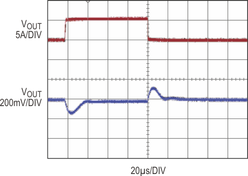
Figure 1 shows the complete schematic for a high efficiency 12 V input to 3.3 V output application. The compact package contains a low 30 mΩ RDS(ON) synchronous bottom MOSFET switch and a 60 mΩ RDS(ON) synchronous top MOSFET switch for high efficiency and minimal thermal issues. Figure 2 shows the continuous and discontinuous conduction mode efficiency and power loss. Discontinuous conduction mode significantly improves light load efficiency while adding a slight increase in output voltage ripple. Figure 3 shows the load-step response with only 330 μF of output capacitance.
 |
||
| Figure 3. | 0 A to 5 A Load Step Response of the Figure 1 Schematic. | |
Dual-Phase Design Increases Output Current Capability
 |
||
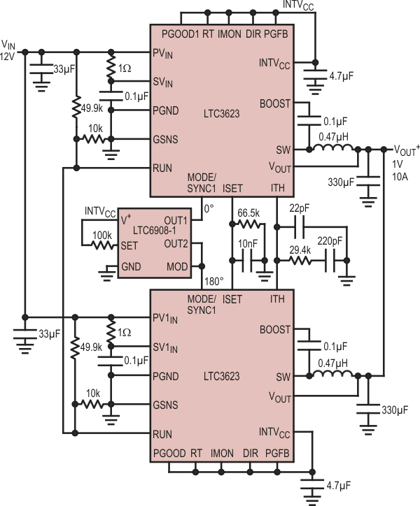
| Figure 4. | 12 V to 1 V at ±10 A 2-Phase Buck Converter. | |
 |
||
| Figure 5. | Efficiency and Power Loss for Application in Figure 4. | |
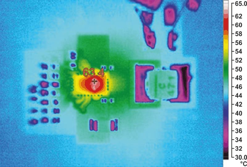
Figure 4 shows a complete 1 MHz 12 V input to 1 V output dual-phase schematic capable of sourcing or sinking up to 10 A. The phases are synchronized by the LTC6908-1 oscillator with 180° interleaving to lower output voltage ripple. Figure 5 shows the efficiency and power loss for the overall system. The low thermal resistance of the LTC3623 package uses the PCB to dissipate heat. The thermal image is shown in Figure 6. From Figure 5, we can see that each phase dissipates 1.8 W at 10 A output current, which raises the chip temperature to 63 °C from an ambient temperature of with no airflow.
 |
||
| Figure 6. | Thermal Image of the Master Phase of the Figure 4 Circuit at 10 A with 0 LFM Airflow at 25 °C Ambient Temperature (38 °C Temperature Rise). |
|
Conclusion
The LTC3623 step-down regulator enables compact POL solutions that can source or sink 5 A without significant thermal mitigation. Power capability is easily expanded by paralleling devices, which has other benefits such as spreading the heat and reducing output ripple. Heat dissipation problems are minimized by the LTC3623’s low thermal impedance and high efficiency capability. The LTC3623’s extensive set of programmable features satisfies the requirements of a wide range of applications.
