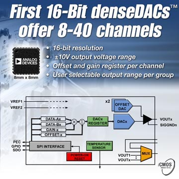
New digital-to-analog converters leverage ADI's iCMOSTM process technology to offer higher levels of precision and programmability in a compact footprint.
Analog Devices, Inc. is introducing eight multi-channel monolithic digital-to-analog converters (DACs) that pack the highest concentration of analog signal processing performance in a single device to resolve design challenges in industrial and instrumentation applications, which demand high precision in small spaces. Developed using Analog Devices’ patented iCMOS process technology, the new DACs extend the company’s denseDAC™ family of high-density converters, combining up to 40 channels, high accuracy, and ±10V output range, in a compact (9 mm x 9 mm) footprint. New programmable on-chip features, such as calibration registers (to compensate for signal errors) and automatic shutdown, ensure system reliability in harsh, high voltage industrial environments, while simplifying board layout. These devices satisfy the needs of today’s systems designers trying to squeeze more and more functionality into smaller board space, particularly in ATE (pin-electronics), optical networking (switches, VOAs) and precision instrumentation applications (oscilloscopes, data generators, industrial I/O cards).
The AD5362 denseDAC is the industry’s first 8-channel DAC with bipolar voltage outputs, 16 bit differential nonlinearity (DNL) and 14-bit integral nonlinearity (INL). In addition, the new DAC incorporates individual user-programmable offset and gain registers per channel, enabling board designers to calibrate their systems and compensate for signal errors that may occur elsewhere in the signal chain. A 50 MHz SPI-compatible serial interface offers group addressing, facilitating fast updating of multiple DAC channels. It also offers flexible diagnostic features, including readback and packet error checking (PEC).
Additionally, the programmable output span of the AD5362 allows users to assign different voltage ranges to different output pins within a 20 V span (the nominal output range is ± 10 V). This gives designers greater freedom to customize industrial products, such as PLC I/O cards, where the ability to provide selectable voltage output ranges previously required the added expense and design complexity of external analog circuitry. The AD5362 also includes a temperature sensor, a thermal monitor mode, a voltage monitor multiplexer, and a power-down mode—all of which are useful in system monitoring.
The AD5362 is available in an 8 mm x 8 mm 56-lead LFCSP package. Other members of the pin-compatible AD536x family offer higher channel (16-channel) or lower resolution (14-bit) alternatives.
About the AD5370 Multi-channel DAC
The AD5370 is a 40-channel DAC offering 16-bit DNL and 14-bit INL, thereby providing the channel density and performance required by manufacturers of high-precision automated test equipment (ATE), optical networking, and industrial and instrumentation (I&I) applications. Its small (9 mm x 9 mm) package offers a reduced footprint for cost- and space-constrained applications without compromising throughput. In addition to a 50MHz SPI-compatible serial interface, the new DAC offers user-programmable offset and gain registers for easier and more precise system calibration, as well as a programmable 20 V output span to provide flexibility in customizing voltage output levels. For even greater addressing flexibility, the device is divided into five groups of eight DACs. A separate input pin is also provided for each group to enable remote ground sensing. Furthermore, the AD5370 has two Vref pins and two offset DACs, enabling the user to set different output voltage ranges.
Pricing and Availability
The AD536x and AD537x DACs are sampling now, with full production quantities available beginning June 2006.
| Part Number | No. of DAC channels | Resolution | Packaging | 1K Per-Unit Price |
| AD5360 | 16 | 16-bit | 8 mm x 8 mm 56-LFCSP 10 mm x 10 mm 52-LQFP |
$29.90 |
| AD5361 | 16 | 14-bit | 8 mm x 8 mm 56-LFCSP 10 mm x 10 mm 52-LQFP |
$27.50 |
| AD5362 | 8 | 16-bit | 8 mm x 8 mm 56-LFCSP 10 mm x 10 mm 52-LQFP |
$23.90 |
| AD5363 | 8 | 14-bit | 8 mm x 8 mm 56-LFCSP 10 mm x 10 mm 52-LQFP |
$19.50 |
| AD5370 | 40 | 16-bit | 9 mm x 9 mm 64-LFCSP 10 mm x 10 mm 64-LQFP |
$62.90 |
| AD5371 | 40 | 14-bit | 10 mm x 10 mm 100-CSPBGA 12 mm x 12 mm 80-LQFP |
$58.50 |
| AD5372 | 32 | 16-bit | 10 8 mm x 8 mm 56-LFCSP 10 mm x 10 mm 64-LQFP |
$52.90 |
| AD5373 | 32 | 14-bit | 10 8 mm x 8 mm 56-LFCSP 10 mm x 10 mm 64-LQFP |
$47.50 |
About ADI’s iCMOS Process
The result of significant, multi-year R&D investments, Analog Devices’ iCMOS industrial manufacturing process technology combines high-voltage silicon with submicron CMOS (complementary metal oxide semiconductor) and complementary bipolar technologies. It enables the development of a wide range of high-performance analog ICs capable of 30-V operation in a smaller footprint, which no other generation of high-voltage parts has been able to achieve. Unlike analog ICs using conventional CMOS processes, iCMOS components can tolerate high supply voltages, while providing increased performance, dramatically lower power consumption, and reduced package size.
