Bipolar junction transistors transfer a current from a lower-resistance emitter to a higher-resistance collector. You can use this property to measure inductance
Bipolar junction transistors transfer a current from a lower-resistance emitter to a higher-resistance collector. You can use this property to measure inductance by connecting a series inductance/resistance circuit in the emitter and biasing on the transistor long enough for the current to reach a maximum value that is at least five LR time constants. When the transistor’s off time is equal to its on time but is still biased by a silicon diode, the LR current decays exponentially toward 0A. Using the transistor’s current-source property, you can measure this current without hindering the decay process in the LR circuit.
The transient analysis of an LR circuit shows that if, during the off time, the LR circuit’s current reduces to a sufficiently low value, say 5% or less, then, for the on time plus the off time, the average current is directly proportional to the value of the inductance. You can control the currents through the transistor and an LR network using timed switching circuitry.
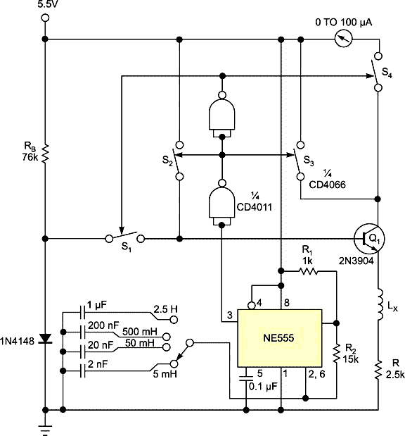
In an inductance-measuring circuit (Figure 1), the NE555 connects as an astable multivibrator oscillator to produce a square wave of approximately 50% duty cycle at frequencies of approximately 46 Hz, 230 Hz, 2.3 kHz, and 23 kHz, depending on the position of the range-selector switch. These values correspond to a full-scale inductance-measurement range as high as 2.5H, 500 mH, 50 mH, and 5 mH. This square wave toggles four quad-packaged CD4066 switches alternately through a pair of CD4011 NAND inverters such that, during the on time, S2 and S3 are closed when S1 and S4 are off, and, during the off time, S2 and S3 are open when S1 and S4 are on.
 |
|
| Figure 1. | In this inductance-measuring circuit, the NE555 connects as an astable multivibrator oscillator to produce a square wave of approximately 50% duty cycle at frequencies of approximately 46 Hz, 230 Hz, 2.3 kHz, and 23 kHz, depending on the position of the range-selector switch. |
At the start of the on time, S2 and S3 are closed, biasing Q1 on from the 5.5V power rail, and the diode and meter disconnect through S1 and S4. After the current in the inductor under test, LX, has exponentially reached maximum as the resistance determines, the off-time half of the cycle begins. S2 and S3 open to remove the 5.5V bias, and S1 and S4 close to insert the meter in the collector-current path and place a small diode-drop bias voltage on the Q1 base.
Normally, the diode’s bias voltage is a bit too low to keep Q1 on. As LX maintains the initial current, however, it drives the emitter negative to temporarily keep Q1 on during the current decay. Most of the exponentially decaying LR current flows through the collector to the meter, and a small portion flows through the base and the bias resistor RB, depending on the Q1 current gain. The meter responds to the current average over the entire on- and off-time cycle due to the mechanical damping of the meter pointer. In this simple circuit, the meter deflection is directly proportional to inductance. With the values in the figure, the meter indicates approximately fullscale 100 μA when measuring a 5-mH inductor on the 5-mH range selection.
At the end of the off-time, the current through the inductance is almost 0A. This appendix shows the current waveform and additional details, such as accounting for high inductor resistance and meter-scale factor.
Editor's Notes:
The NE555 high output appears slightly lower than the specified valid logic 1 voltage for the CD4011, but is still well above the switching threshold and is driving zero load current.
The meter resistance has not been specified; the author used a moving pointer bench VOM. A digital meter may not work properly unless it has the ability to average a pulsed signal.
Q1 is biased just below threshold. While the data sheets indicate a 1N4148 diode has typically lower forward voltage drop than the 2N3904 VBE, there is a possibility that certain combinations of diode and transistor may bias the transistor on during tOFF and cause additional meter deflection. It might be necessary to hand-pick these components.
Remember to ground any unused input pins on the remainder of the CD4011 quad NAND package.
APPENDIX for Inductance Meter
First the evolution of current through the L-R circuit is considered. The current at a time t in the L-R circuit is
 |
(1) |
where
 |
is the maximum current achieved at time t = tON. By considering the values of the components associated with NE555 we see that tON ~ 20μs when set for measuring a maximum inductance of 5mH. For this setting the maximum value of R/L that is possible is 2,500/0.005 = 500,000. So we see that at t = tON the exponential term in (1) is almost 0 as (RtON/LX) = 10. This means i = i0 at t = tON.
Next we consider the decay of current during tOFF . The current at time t in the L-R circuit once it starts decay is given by
 |
(2) |
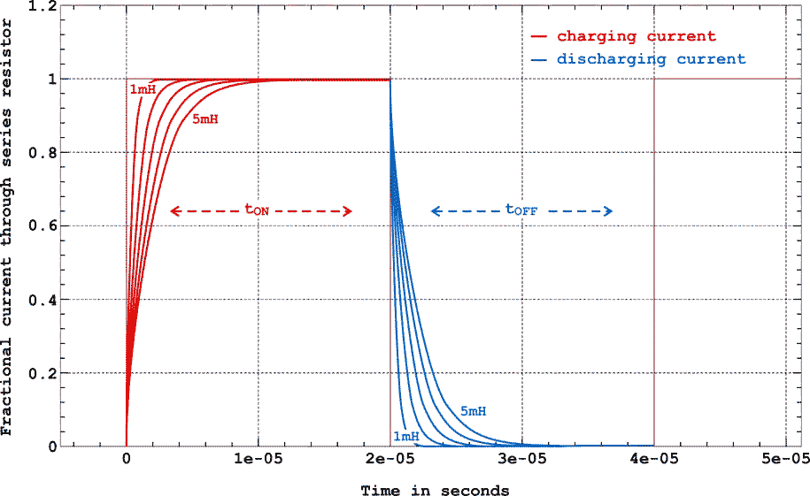
Since tOFF ~ tON we see from the previous argument that i = 0 at t = tOFF. The plots of evolution/decay of currents in the L-R circuit have been shown in Figure 2.
 |
|
| Figure 2. | Timing diagram of evolution of currents for different values of LX (1-5mH), R=2.5kΩ. |
The timing diagram (Figure 2) clearly indicates that the current at the end of tON would have reached the maximum value or it would have decayed to 0 at the end of tOFF. So the average current through the meter can be calculated as,
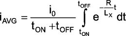 |
(3) |
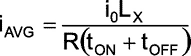 |
(4) |
We see that the average current is directly proportional to the value of the inductance LX . Since tON is approximately = tOFF by the choice of R1 and R2 for the NE555, to measure different values of inductances it is sufficient to change the capacitor associated with the NE555. To double the range of inductance measurement the value of this capacitor has to be simply doubled as has been shown in Figure 2 above.
The inductance will also have an associated resistance with it which comes due to the length/thickness of the wire. This can be accounted by modifying (4) as,
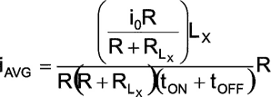 |
(5) |
or
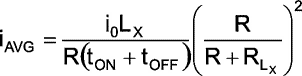 |
(6) |
which is essentially multiplying the actual inductance by the factor
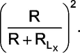 |
The manipulation in (5) is that due to the introduction of extra resistance RLx with LX the peak current to which the inductance is driven has reduced from i0 to i0R/(R+RLx). Next in the denominator R has to be replaced by (R+RLx). To rewrite and retain the form of (4) we throw an extra R in the numerator and denominator and rearrange into (6). RLx can be measured separately using a resistance meter. R is known to be 2.5kΩ as per this design. It should be noted that R can be changed to 5kΩ resulting in the modified range of 0-10mH instead of 0-5mH. The timing plots would still be the same with 5mH curve indicating the one for 10mH, but the peak current i0 would be halved. Further R may have to be calibrated slightly to get the right value of inductance. The actual inductance is obtained as the observed inductance multiplied by the inverse of the above mentioned factor i.e,
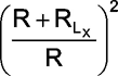 . . |