A capacitor that you charge through a resistor operates at 50% efficiency; hence, many engineers avoid using switched-capacitor dc/dc converters. That efficiency figure holds true only for capacitors with no initial voltage, however. If you decide to switch a precharged capacitor, you can transfer energy to an output with a power-efficiency approaching 100%.
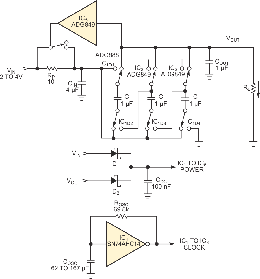
To attain a four-thirds multiple of an input supply voltage, you can charge three capacitors to one-third of each supply voltage and then add that one-third of the input voltage to the input voltage to yield an output voltage that is four-thirds of the input voltage. You series-connect three capacitors of equal value and then charge this series string to a voltage equal to the input voltage. Because the values are equal, each of the capacitors charges to one-third the input voltage. The circuit then connects these three capacitors in parallel on top of the input voltage and switches this increased voltage to the output (Figure 1). The circuit repeats these two phases of operation at clock frequency F.
 |
||
| Figure 1. | This charge-pump circuit raises the input voltage to a 1.33 multiple. You can use it as a 2.5-to-3.3 V converter. The circuit works in environments with high magnetic fields that might interfere with an inductor-based converter. |
|
CIN and COUT are filtering capacitors at the input and output, respectively. RP is a protective resistor, which limits the inrush current to the capacitors at power-on. As the output voltage rises, it closes IC5 and shorts out this resistor. Schottky diodes D1 and D2 allow you to power the ICs using the input voltage until the output rises, at which time the higher output voltage powers the ICs. CDC is a storage and decoupling capacitor for this power bus. The higher power-supply voltage is necessary for proper operation, and it lowers the on-resistance of the analog switches. The 0.4 Ω on-resistance of IC1 results in low circuit losses and high-efficiency operation. IC1, IC2, and IC3 exhibit a break-before-make operation, which is essential in this case.
For a 50%-duty-cycle clock, you can calculate the theoretical power-efficiency of the converter, according to the following equation:
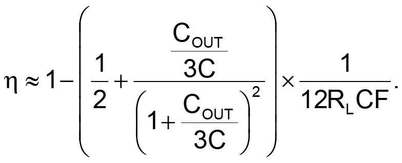
If the value of COUT is equal to the value of C, the power loss due to charging of the three capacitors is about two-thirds of the power loss during the discharging phase. The power consumption of the control circuit reduces the efficiency of this calculated value. For CMOS circuits, the power consumption rises linearly with the operating frequency. By choosing the operating frequency, you can optimize the efficiency of the circuit. The optimum frequency is inversely proportional to the load resistance, RL. Fortunately, the efficiency maximum is flat, so you can achieve efficiencies higher than 90% over a wide range of values for RL. You can attain 94% efficiency driving a 120 Ω load over clock frequencies of 100 to 400 kHz. If you set a 229-kHz operating frequency, an input of 2.2 V yields a 2.87 V output at an efficiency of 95.9%. The optimum clock frequency shifts to lower values at lighter loads. You can drive a 269 Ω load at 100 kHz and achieve an output of 2.88 V.