Many power applications ranging from luminescent and fluorescent lighting to telephone-ringing voltage generators require a more or less sinusoidal-drive voltage. These applications typically require a waveform of only moderate quality, and its frequency isn't especially critical. However, avoiding waveform discontinuities that cause unwanted current peaks, excessive device dissipation, and EMC problems rules out using filtered square waves or other stepped waveforms. Sometimes, a trapezoidal drive may be acceptable but it's only a second choice at best. This Design Idea proposes a method of generating sine waves that offers a number of advantages over more complex methods:
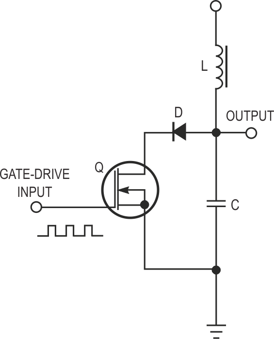
The circuit requires only one power-switching device, and you can use an analog or a digital signal to drive the switching device. The circuit also requires only a few components: a diode, a switching transistor or a MOSFET, an inductor or a transformer, and a capacitor. Further, the design's circuit losses are low, and the switching device experiences minimal stress during operation. Figure 1 shows the basic circuit, and Figure 2 illustrates waveforms within the circuit.
 |
||
| Figure 1. | Few components are necessary to produce a pseudo sine wave. |
|
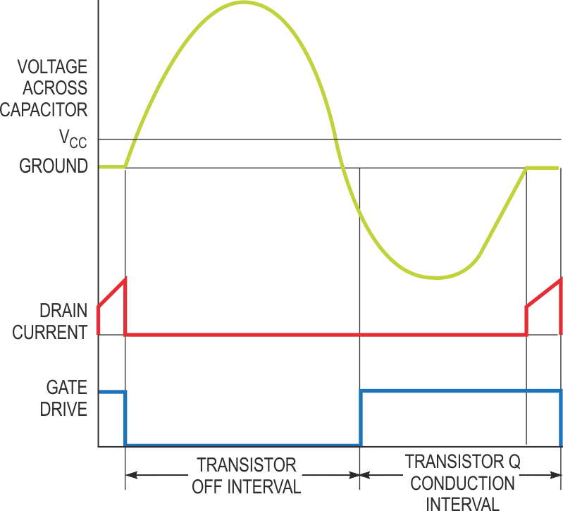
In operation, the sine-wave output appears across inductor L in a series LC circuit. An external clock source produces gate drive for transistor Q at a frequency that's lower than the LC circuit's natural resonant frequency. When the transistor conducts, the inductor receives a charging current via diode D. When conduction ends, energy stored in the inductor transfers to capacitor C, and a damped oscillation begins (uppermost trace in Figure 2). The voltage across capacitor C approximates a sine wave (top trace). Drain current in transistor Q shows that no current flows until the capacitor voltage forward-biases diode D (middle trace). The gate-drive pulse interval is lower than the series-resonant frequency that L and C present (bottom trace).
 |
||
| Figure 2. | The circuit in Figure 1 produces these waveforms. | |
During the negative-going portion of the cycle, the external clock source applies gate drive to the transistor. Diode D is still reverse-biased, and thus no current flows into Q. When the voltage across C goes positive, diode D conducts and allows current to recharge the inductor and replenish energy lost in the previous cycle. In balanced operation, energy supplied during the conduction phase replenishes energy supplied to the load and dissipated in component losses.
To produce a higher peak voltage, you extend the conduction interval by raising the drive frequency or by extending the on interval. You can regulate the output voltage by applying conventional closed-loop feedback techniques to a variable-frequency clock oscillator or, in digital systems, by altering the clock's duration. For most applications in which load current is relatively fixed, such as in an electroluminescent panel lamp, an open-loop adjustment or manual control offers sufficient flexibility once you determine a clock-frequency range that corresponds to the desired degree of illumination.
For peak voltages not exceeding 10 times the power-supply voltage, you can connect the load directly to the junction of D, L, and C. You can achieve higher voltage-to-step-up ratios at the expense of applying additional voltage and current stress to L and C. Instead, you can add an isolated secondary step-up winding to the inductor. For optimum efficiency, use components designed for high-frequency power handling – for example, a polypropylene-dielectric capacitor and a low-loss inductor.
If the load consists of an electroluminescent panel that behaves as a lossy capacitor, you may be able to eliminate the use of external capacitor C. Transistor Q must obviously be able to withstand peak voltages and currents that the circuit imposes, but its specifications are otherwise relatively noncritical. No switching loss occurs at the beginning of the conduction due to the Class E mode of operation, and the output capacitor assists the device's turn-off recovery. For output voltages not exceeding approximately 50 V, you can improve efficiency by selecting a Schottky or other fast-recovery diode for use in the circuit.
For powering lamps and generating telephone-ringing signals, the sine wave's "flat spots" are of little consequence because of their relatively short duration and low harmonic-energy content. You can minimize these intervals by reducing the LC ratio and thus increasing the loaded Q factor of the LC circuit. However, for a given output voltage, increasing Q factor also increases the peak current because the same amount of energy must transfer to the inductor in less time.