A previously-published Design Idea outlined a polarity protection circuit [1] that provides the correct connection of the battery to a load regardless of the battery’s orientation in its holder. The circuit, based on the MAX4636, a fast-switching, low-voltage, dual SPDT CMOS analog switch IC from Maxim Integrated, was functional, but it had some drawbacks. It had a somewhat limited power-supply voltage range (1.8-5.5 V), and a slightly high internal resistance, which limits its applications to products with modest current loads, not exceeding 30 mA. Fortunately, those limitations can now be overcome, thanks to some significant advances in MOSFET technology.
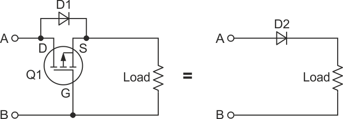
Figure 1 illustrates protection of the load against a reversed-polarity battery using a P-channel MOSFET transistor. Normally, to turn on the P-channel MOSFET, you need to apply the proper voltage to its control gate-source junction (negative potential at the gate terminal and positive potential at the source terminal). The P-channel MOSFET shown in Fig. 1 is connected slightly differently and operates as follows.
 |
||
| Figure 1. | This circuit protects the load against a reversed battery using a P-channel MOSFET. | |
When power is applied to the A and B terminals (A is positive and B is negative), the transistor’s internal diode D1 is forward biased and provides control gate-to-source voltage of Q1, thus turning it on. The MOSFET's low resistance acts as a shunt around diode D1 and feeds current to the load.
When the battery is reversed, the voltage is applied to the A and B terminals (now A is negative and B is positive), and the transistor’s internal diode D1 is reverse biased and the gate-to-source voltage of Q1 is 0. As a result, the Q1 transistor is off and the load gets no current.
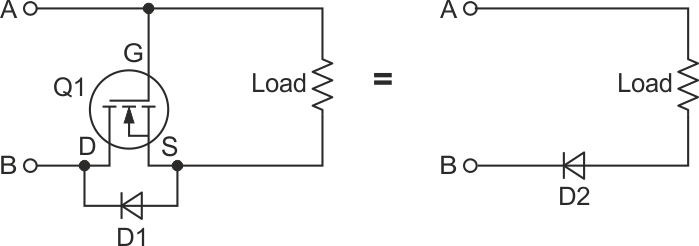
In other words, the P-channel MOSFET Q1 in this circuit behaves like a diode (i.e. a virtual "D2"), with very low forward threshold voltage. An N-channel MOSFET can be used in a similar way (Figure 2).
 |
||
| Figure 2. | The circuit protects the load against reversed battery using an N-channel MOSFET. | |
When A terminal is positive and B terminal is negative, the transistor’s internal diode D1 gets forward bias and provides control gate-to-drain voltage of Q1, thus switching it on. The MOSFET's low resistance shunts the D1 diode, thus feeding current to the load.
When power is applied to the A and B terminals in reverse (A is negative and B is positive), the transistor’s internal diode D1 is reverse biased and the gate-to-source voltage is equal to 0. MOSFET Q1 is turned off and the load gets no current.
The circuits illustrated in Figures 1 and 2 may be used to protect a load against reversed battery instead of an ordinary diode reversed-polarity protection, but cannot supply a load with power if the battery is installed backwards.
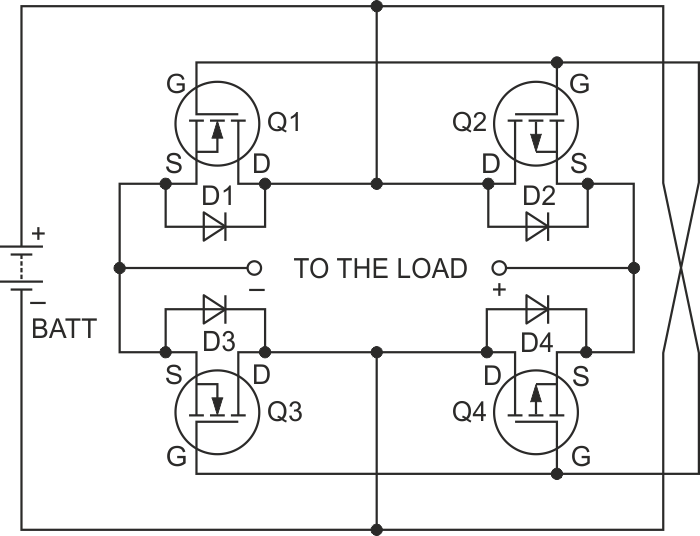
When a battery is installed as shown in Figure 3, positive potential is applied to the source of the P-channel transistor Q2 through its forward biased internal diode D2. This puts Q2's gate at potential of the negative terminal of the battery, thereby turning it on. The battery's negative terminal is connected to the source of the N-channel transistor Q3 through its forward biased internal diode D3. Under these conditions, Q3 turns on because its gate is at the potential of the positive terminal of the battery. Summing up, with the battery in this orientation, Q2 and Q3 are active and carry the battery’s voltage to the load while Q1 and Q4 remain off.
 |
||
| Figure 3. | This circuit provides power to the load with any installation of the battery. | |
In the next scenario, the battery is installed in the opposite orientation. Now, the positive potential is applied to the source of the P-channel transistor Q4 through its forward biased internal diode D4. Since Q4's gate is at potential of the negative terminal of the battery, it turns on. Q1's internal diode D1 is forward biased, allowing it to apply the potential from the battery's negative terminal to the source of the N-channel transistor Q1. Since Q1's gate is at potential of the positive terminal of the battery, Q1 turns on. Since Q1 and Q4 are both on, the battery is connected to the load, while Q2 and Q3 are off.
Note that this design includes a safety feature which makes use of the MOSFETs' internal diodes. The diodes in transistors Q1-Q4 are connected to form a full-bridge rectifier. In case the MOSFETs fail to operate, the diode bridge can still rectify the input, thereby providing power of the proper polarity to the load.
Addendum
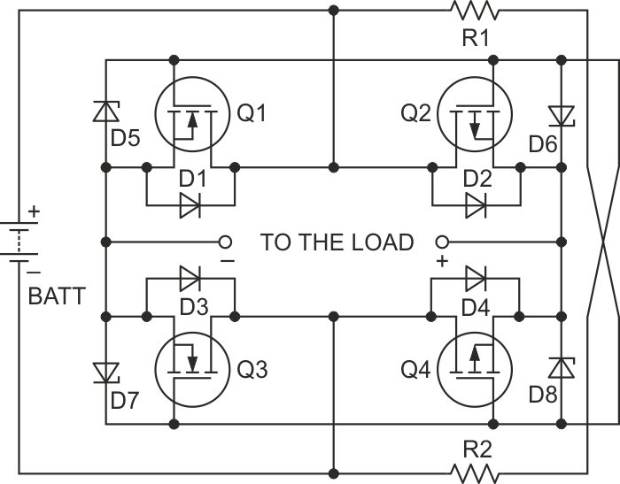
The circuit in shown Fig. 3 is intended for use with relatively low voltages that don't exceed the maximum allowable gate-source junction of the N-channel and P-channel MOSFETs, usually ±15-20 V. For applications requiring a higher battery voltage, the circuit in Fig. 3 should be modified to protect the MOSFETs’ gate-source junctions as in Figure 4.
 |
||
| Figure 4. | Protection of the gate-source junctions of the MOSFETs. | |
The circuit adds zener diodes D5 - D8 to protect the MOSFETs' gate-source junction. Resistors R1 and R2 provide current limiting. In most cases, the value of Vzener (reverse breakdown voltage) for D5 - D8 should be between 12 and 13 V. It’s enough to switch MOSFETs on providing their minimum RDS-ON values. The values of R1 and R2 (R1 = R2 = R) may be calculated as follows:
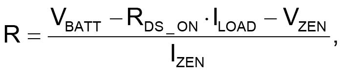
where VBATT is the battery’s voltage, RDS-ON is the drain-source resistance of the switched on MOSFET, ILOAD is the load current, VZEN is the zener diode’s reverse breakdown voltage, and IZEN is the zener diode’s operating current.
