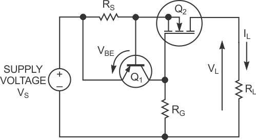
Most readers are familiar with the current-limiting circuit in Figure 1, in which the load current, IL, is limited to a value of
where VBE is the base-to-emitter voltage and RS is the sense resistance. Under normal conditions, in which the base-to-emitter voltage is too small to bias Q1 on, P-channel MOSFET Q2’s gate resistor, RG, biases Q2 fully on, and only the load resistance, RL, and the load voltage, VL, determine the load current. However, if the load current increases to a point at which the base-to-emitter voltage is approximately 0.7 V, Q1 starts to conduct and reduces Q2’s gate-to-source voltage, VGS, to a level that holds the load current roughly constant at a value you derive from
 |
|
| Figure 1. | A conventional two-transistor current limiter prevents excessive current from reaching the load. |
This linear current limiter is effective for applications in which the maximum load current, the supply voltage, or both are relatively small. However, the power that the circuit’s pass transistor, Q2, dissipates limits the circuit’s applicability. For example, if the maximum load current is 200 mA and the supply voltage, VS, is 24 V, a short circuit across the load would dissipate almost 5 W into Q2. Q2 must handle this power with adequate margin, and additional heat-sinking may be necessary to keep its junction temperature at a safe level. Using larger values of maximum load current, supply voltage, or both exacerbates this problem. In many applications, the cost, size, and weight of the components necessary to handle the short-circuit power dissipation may be prohibitive.
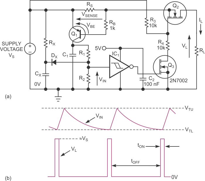
However, by adding a few inexpensive components, you can adapt the circuit to provide effective current limiting with none of the power-dissipation headaches. The resulting circuit functions as a self-resetting circuit breaker (Figure 2a). Again, Q1 and RS provide a current-monitoring function in which the sense voltage VSENSE = IL × RS. In this circuit, however, Q2 is either fully on or fully off and never biases into its linear region. Because Q1’s base current is normally small, the voltage drop across base resistor RB is also small, such that the base-to-emitter voltage is approximately equal to the sense voltage.
 |
|
| Figure 2. | Adding a few components turns the current-limiting circuit into a pulser that reduces heat in the pass transistor, Q2 (a). The circuit’s waveforms show the relationship between the input voltage and the load voltage (b). |
To understand how the circuit works, assume that the load current is initially low and the base-to-emitter voltage is less than 0.7 V. Under these conditions, Q1 is off and timing capacitor C1 remains uncharged such that VIN, the voltage at the input of Schmitt inverter IC1, is 0 V. Thus, IC1’s output is approximately 5 V, biasing Q3 on, which in turn provides gate bias for Q2 through R4, allowing current to flow from the supply voltage into the load through the sense resistor and Q2’s on-resistance.
If a fault now causes the load current to increase to a level at which the base-to-emitter voltage is approximately 0.7 V, Q1 turns on and its collector current rapidly charges C1. The input voltage now quickly rises toward the Schmitt inverter’s upper threshold voltage, VTU, at which point IC1’s output goes low, turning off Q3 and Q2. The load current now falls to 0 A and the base-to-emitter voltage falls to 0 V, thereby causing Q1 to turn off. C1 now begins to discharge through R1 and R2, and the input voltage slowly falls toward the Schmitt inverter’s lower threshold voltage, VTL. At this point, IC1’s output again goes high, Q3 and Q2 turn on, the circuit breaker resets itself, and the process repeats until you remove the fault.
The circuit’s waveforms show the relationship between the input voltage and the load voltage (Figure 2b). Because load current flows into Q2 only during the on-time, the average power it dissipates is directly proportional to the duty cycle:
where PAVG is the average power in watts, tON is the on-time, and tOFF is the off-time. Provided that C1, R1, and R2 set a large enough time constant, the off-time will normally be much greater than the on-time, and the resulting power that Q2 dissipates will be low. Like the linear-current limiter, the sense resistor sets the circuit breaker’s current limit:
R1 and R2 form a potential divider that ensures that the input voltage can never exceed IC1’s maximum input voltage. Select values such that the input voltage is 5 V or less when Q1 is fully on, where the voltage of C1 is roughly equal to the supply voltage. Also, choose values that are large enough to provide a large time constant without requiring an excessively large value of C1. The selection of transistor Q1 isn’t critical, but you should select a device with good current gain and make sure that its maximum collector-to-emitter voltage is greater than the supply voltage. When choosing a P-channel MOSFET for Q2, remember that it must withstand the full supply voltage when you bias it off, so make sure that the maximum drain-to-source voltage is greater than the supply voltage. When choosing a value for the sense resistor, ensure that the base-to-emitter voltage is less than 0.5 V at the maximum normal value of the load current.
Loads such as filament bulbs, capacitive loads, and motors that exhibit a large inrush current can cause the circuit breaker to trip on power-up. You can avoid these problems by adding capacitor CX, diode DX, and resistor RX. On power-up, CX is initially uncharged and pulls the input voltage toward 0 V through DX. This action prevents the circuit breaker from tripping until the inrush current subsides. CX and RX determine a delay, after which the voltage on CX eventually rises to the supply voltage, DX becomes reverse biased, and the circuit breaker is then free to respond to overcurrent faults. Be prepared to experiment with the values of CX and RX to get the right delay time. Values of 10 µF and 1 MΩ, respectively, are good starting points.
