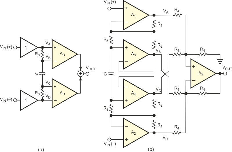
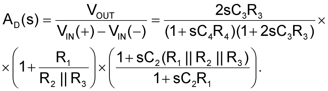
Modern battery-cell voltages of 3 to 3.6 V require circuits that offer efficient low-voltage operation. This Design Idea proposes an ac-coupled instrumentation-amplifier design that features high CMRR (common-mode-rejection ratio), wide dc input-voltage tolerance, and a first-order highpass characteristic. Most of these features stem from a high-gain first-stage design. The circuit uses popular-value and -tolerance components. Figure 1a shows the simplified amplifier circuit. The general principle is that the capacitor, C, and the R3 resistors buffer and ac-couple the input signal. The second stage comprises two differential amplifiers, AD. Each of them amplifies half the differential input signal. A summing operation yields the following expression for VOUT:
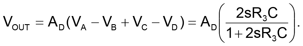
In Figure 1a, VA, VB, VC, and VD are the two differential amplifiers' inputs, and AD is the gain. The time constant 2R3C defines the highpass cutoff frequency. Figure 1b shows the detailed circuit. The input stage comprises op amps A1, A2, A3, and A4. A1 and A2 are the main gain stages. Because their inverting and noninverting inputs are at the same potential, the input voltages supply the R3 resistors. The buffers A3 and A4, along with the R2 resistors, produce an amplification factor, 1 + R3/R2, for the current in R3, because R2 and R3 connect to equal potentials. This circuit structure is the heart of the design. The voltage on capacitor C has no ac component, and A1 and A2 each amplifies one-half of the differential-input ac signal. C filters the input dc component, which appears at the A3 and A4 outputs. The second stage is a unity-gain, four-input adder-subtracter stage. It implements the above equation, where
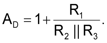
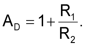
Assuming R3 >> R2,
 |
|
| Figure 1. | Capacitor C ac-decouples the simplified amplifier circuit (a); the detailed circuit (b) uses gain stages and an adder-subtracter stage. |
Another possible implementation for the second stage could use two differential-channel ADCs, producing a digitized VOUT, ready for microcomputer processing. If a ±5 V supply is available, it is possible to obtain VOUT by using two difference amplifiers on one chip, such as the INA2134. You can calculate the minimum CMRR as:
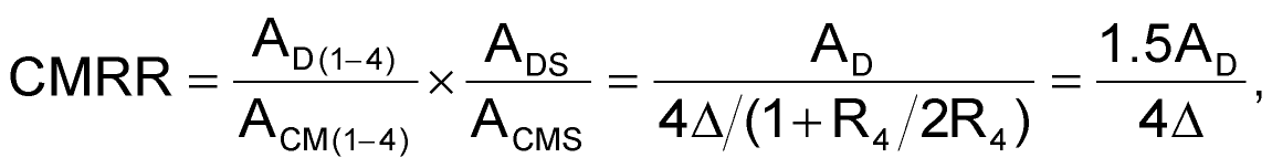
where AD(1-4) is the differential gain of amplifiers A1 through A4, ACM(1-4) is the common-mode gain of these amplifiers, AD5 is the differential gain of amplifier A5, and ACM5 is the common-mode gain of A5. Δ is the tolerance of the R4 resistors in the circuit. A very important parameter is the op amps' input offset voltage, especially for A3 and A4. The A1 and A2 offsets do not contribute to error, because they add to the input signal's dc component, which capacitor C cancels. The maximum output-voltage error attributable to op-amp offset voltage is:
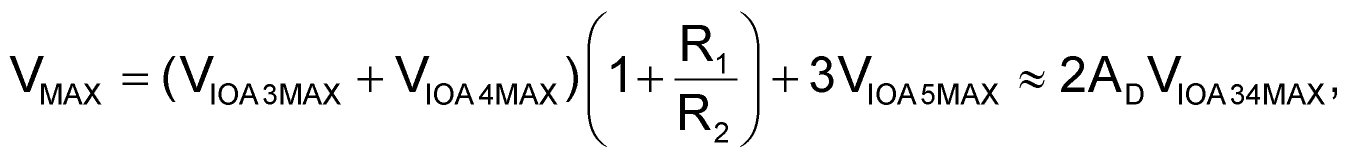
where VIOMAX are the maximum offset voltages of the corresponding op amps. In selecting op amps, you should note the following: A3, A4, and A5 should be low-offset and high-CMRR types, and A1 and A2 should have high open-loop gain, CMRR, and gain-bandwidth products. Figure 2 shows a practical amplifier circuit. The power supply is one 3 V lithium battery. You can use several op-amp types, such as MCP607s or OPA2336s. Because of the input common-mode voltage range, you set the signal ground to one-third of the supply voltage. The D1 diodes prevent the circuit from latching up. The R7-C4 networks provide RF-noise filtering at the inputs. You derive the network's values from the following consideration: With
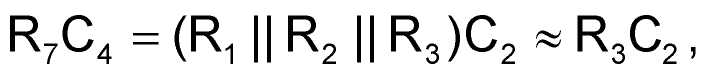
the high-frequency zero in the amplifier's transfer function cancels:
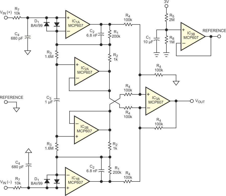 |
|
| Figure 2. | This high-CMRR instrumentation amplifier operates from extremely low supply voltages. |
The circuit has the following advantages:
- The first stage ensures the overall gain, thus providing high CMRR without the use of high-precision resistors in the second stage.
- By connecting the low-frequency-determining RC network to the inverting inputs of the op-amp pair that amplifies the input signal, the circuit needs no additional input buffers.
- The circuit delivers a standard, first-order highpass characteristic, using passive components with popular values and tolerances.
- The differential-input range is as high as 2 V, using a 3 V supply.
- The circuit consumes low supply current and power: approximately 120 μA, 0.4 mW.
