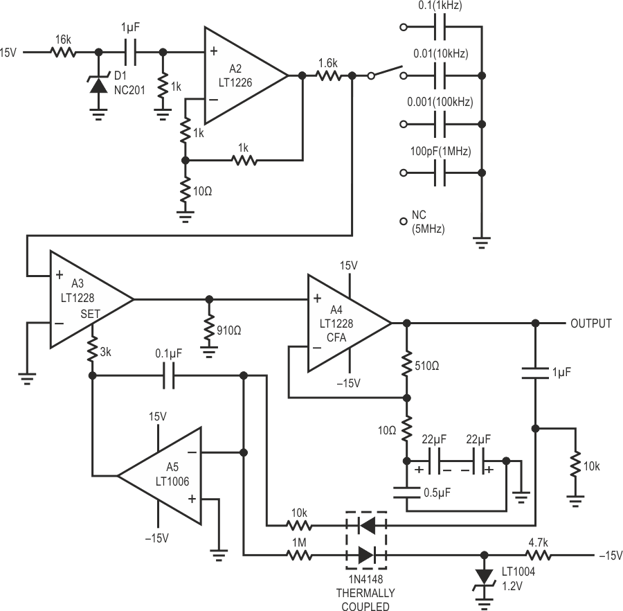
Filter, audio, and RF-communications testing often require a random noise source. Figure 1’s circuit provides an RMS-amplitude regulated noise source with selectable bandwidth. RMS output is 300 mV with a 1 kHz to 5 MHz bandwidth, selectable in decade ranges.
 |
|
| Figure 1. | Broadband random noise generator uses gain control loop to enhance noise spectrum amplitude uniformity. |
Noise source D1 is AC coupled to A2, which provides a broadband gain of 100. A2’s output feeds a gain control stage via a simple, selectable lowpass filter. The filter’s output is applied to A3, an LT1228 operational transconductance amplifier. A3’s output feeds LT1228 A4, a current feedback amplifier. A4’s output, also the circuit’s output, is sampled by the A5-based gain control configuration. This closes a gain control loop to A3. A3’s set current controls gain, allowing overall output level control.
 |
|
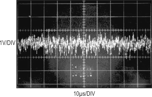
| Figure 2. | Figure 1’s output in the 1 MHz filter position. |
 |
|
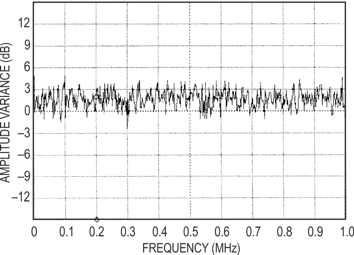
| Figure 3. | Amplitude vs frequency for the random noise generator is essentially flat to 1 MHz. |
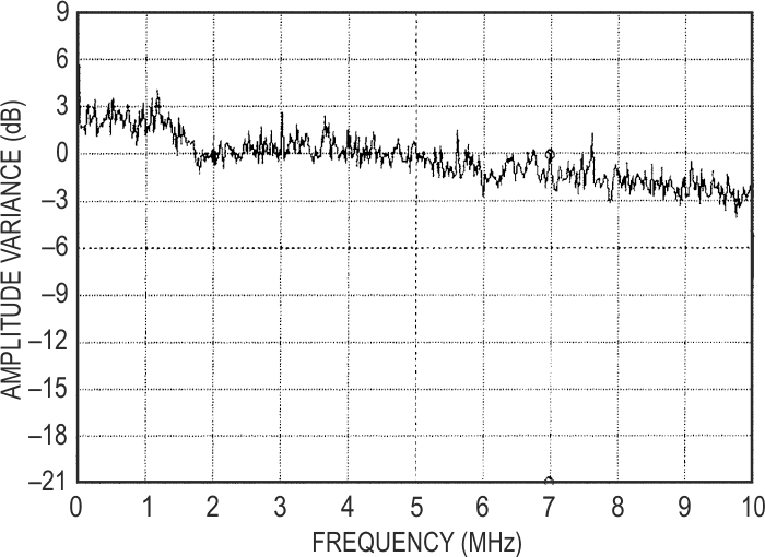
Figure 2 shows noise at 1 MHz bandpass, with Figure 3 showing RMS noise versus frequency in the same bandpass. Figure 4 plots similar information at full bandwidth (5 MHz). RMS output is essentially flat to 1.5 MHz with about ±2 dB control to 5 MHz before sagging badly.
 |
|
| Figure 4. | RMS noise vs frequency at 5 MHz bandpass shows slight fall-off beyond 1 MHz. |
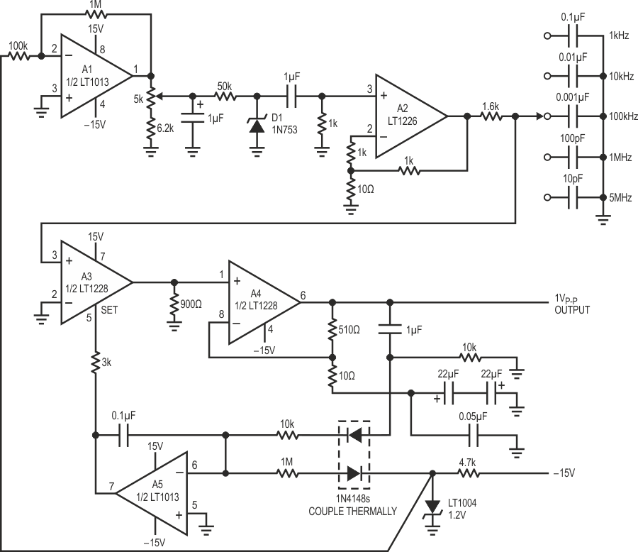
Figure 5’s similar circuit substitutes a standard zener for the noise source but is more complex and requires a trim. A1, biased from the LT1004 reference, provides optimum drive for D1, the noise source. AC coupled A2 takes a broadband gain of 100. A2’s output feeds a gain-control stage via a simple selectable lowpass filter. The filter’s output is applied to LT1228 A3, an operational transconductance amplifier. A3’s output feeds LT1228 A4, a current feedbacks amplifier. A4’s output, the circuit’s output, is sampled by the A5-based gain control configuration. This closes a gain control loop back at A3. A3’s set input current controls its gain, allowing overall output level control.
 |
|
| Figure 5. | A similar circuit uses a standard Zener diode, but is more complex and requires trimming. |
To adjust this circuit, place the filter in the 1 kHz position and trim the 5k potentiometer for maximum negative bias at A3, pin 5.