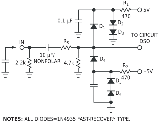
You typically accomplish overvoltage or surge protection at circuit inputs by connecting diodes to the supply rails, connecting zener diodes to ground, or connecting transzorbs to ground. Unfortunately, for high-energy surges at the inputs, connecting diodes to the supply rails results in surges in supply lines and affects other components because of the inductance of supply rails, regulator shutdown, and so on. Zener diodes have limited surge capability, and transzorbs have large capacitance and are therefore suited only for low-bandwidth applications.
The circuit in Figure 1 has many advantages over these approaches: wide bandwidth and low capacitance; high surge-energy handling because the diodes can carry 50 A peak; 1 A continuous current; and fast response. Also, the circuit doesn't affect the supply rails and is suitable for protecting multiple I/O lines because the lines can share the bias voltage. You can further improve the response time by using faster diodes; a ground plane; low-inductance, short connections; and close, high-frequency decoupling.
 |
|
| Figure 1. | Two surge shunt paths, consisting of D1, D2, and D3 to ground or D4, D5, and D6 to ground, provide overvoltage protection. |
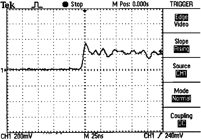
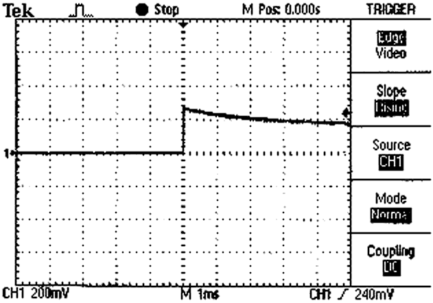
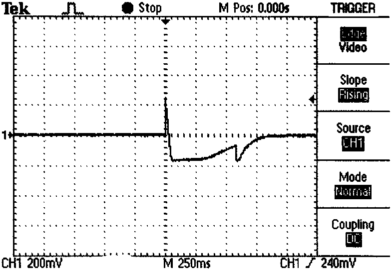
The circuit reverse-biases D1 and D4 to bias voltages of ±1.2 V, respectively. R1 and R2 bias two pairs of diodes, D2/D3 and D5/D6, respectively, to generate the ±1.2 V. R1 and R2 prevent input surges from reaching the supply rails. The surge shunt path consists of D1, D2, and D3 to ground or D4, D5, and D6 to ground, depending on the surge's polarity. Because of the ±1.2 V bias-voltage settings, the circuit works with maximum input signals of ±1 V. Above this level, D1 and D4 start to leak and distort the signal. The circuit was tested using a 100-µF/50 V test capacitor charged to 30 V and then discharged to the input. A DSO captured the results (Figure 2). In Figure 2a, with RS = 100 Ω, the peak is approximately 3.5 V, and settling to around 2 V occurs within 15 nsec. Figure 2b shows the same response as Figure 2a but with a horizontal scale of 1 msec/div. Figure 2c is also the response under the same conditions but shows the long-term response and the coupling-capacitor recovery. If you let RS = 0, the peak rises to 10 V and settles within 500 nsec. Thus, some small resistance, such as 100 Ω, is necessary for RS.
|
|||||||
| Figure 2. | Tests with a 30 V charged capacitor at the input show the circuit’s response with a horizontal scale of 25 nsec/div (a) and 1 msec/div (b). The long-term response shows the recovery of the coupling capacitor (c). |
||||||