Powering portable telemetry systems for long-term monitoring presents interesting design challenges. Batteries are unsuitable for certain critical applications, and, in these circumstances, designers typically use wireless inductive links to transmit both power and data. An inductive link comprises an RF transmitter that drives a fixed primary coil, and a loosely coupled secondary coil that supplies power to the portable circuitry. For design engineers, measuring transmitted power takes on considerable importance because it imposes limits on the amount of circuitry that designers can include in the portable circuitry. Unfortunately, classical test equipment is poorly suited to the task. Standard voltage probes pick up noise that the primary coil induces, and, in some applications, the portable circuits are hermetically encapsulated in small enclosures that prevent entry of a cable or a probe.
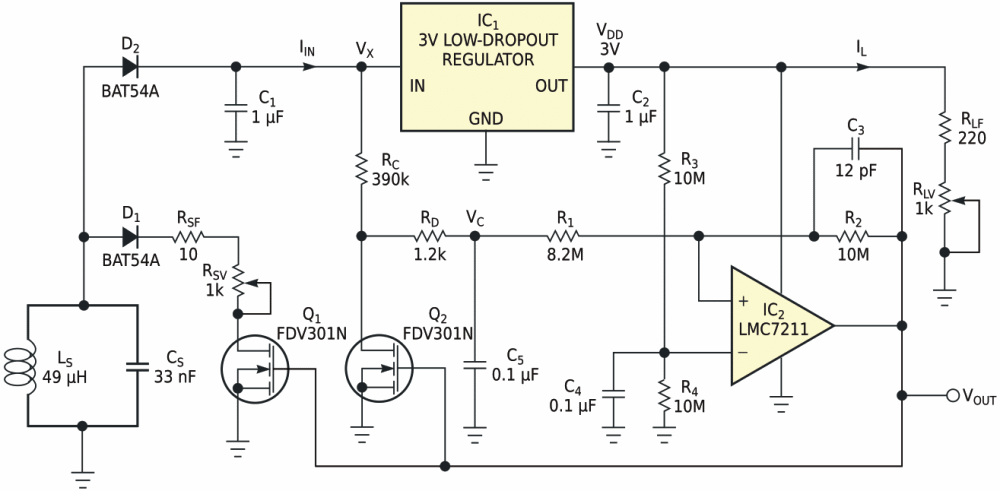
The circuit in Figure 1 reduces noise effects because its VFC (voltage-to-frequency converter) produces a PPM (pulse-position-modulated) output signal, VOUT, that integrates, or averages, noise. In addition, the design uses “load modulation” to eliminate wired connections. When the PPM signal drives on MOSFET switch Q1, the switch connects an additional loading network comprising D1 and the series combination of RSF and RSV across the secondary coil, LS. A load-modulation receiver connects to the primary coil and recovers the PPM signal. When you build it with surface-mounted components, the VFC circuit occupies a board area of only 238 mm2.
 |
|
| Figure 1. | A low-power VFC and load modulator measure power generated by a wireless-telemetry power source. |
To understand the circuit's operation, assume that a 125-kHz sinusoidal magnetic field induces approximately 4 to 16 V in secondary coil LS. To improve power-transfer efficiency, LS and CS form a tuned, 125-kHz tank circuit having a loaded Q factor, QL, of approximately 8. Schottky diode D2 rectifies the voltage induced in LS, and C1 provides lowpass filtering. The resultant dc voltage, VX, powers low-dropout regulator IC1, which supplies a constant 3 V to VFC IC2 and the load resistors, RLF and RLV. Trimmer potentiometer RLV sets the output current at 2.5 to 13.5 mA.
The combined total current drain of the low-dropout regulator and the VFC measures a few tens of microamperes and is negligible compared with the output current. Hence, IIN approximately equals IL. Equation 1 expresses the dc output power that the inductive power supply produces:
 |
(1) |
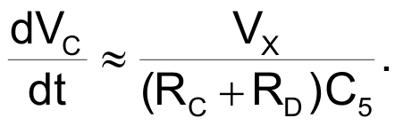
This equation shows that the output current is constant and therefore the dc output power, PX, is proportional to the dc voltage, VX. After setting a known initial output current adjustment via RLV, you can test the inductive power supply's output ability by measuring the transmitted dc voltage that the VFC digitizes. To minimize power consumption, component count, and pc-board area, a simple passive integrating network comprising RC, RD, and C5 replaces the classical op-amp integrator that constitutes a typical VFC's input stage.
The VFC generates a constant-amplitude sawtooth voltage whose rising slope is proportional to VC across integrating capacitor C5. When the capacitor's voltage reaches a high reference voltage, switch Q2 rapidly discharges the capacitor to a low reference voltage. This action produces a free-running waveform whose frequency is proportional to the input voltage, VX. A noninverting Schmitt trigger comprising comparator IC2; its positive-feedback network, R1, R2, and C3; and supply-voltage splitter R3, R4, and C4 defines the high- and low-level reference voltages, as equations 2 and 3 calculate.
 |
(2) |
 |
(3) |
Equation 3 shows that, to reset the integrated voltage almost to 0 V, the value of R1 must be slightly lower than that of R2. Using standard values of E12-series resistors and taking into account power- consumption constraints, select a value of 8.2 MΩ for R1 and 10 MΩ for R2. Replacing these values in equations 2 and 3 yields, respectively:
 |
(4) |
To understand the VFC's operation, assume that, at start-up, capacitor C5 is fully discharged. Consequently, comparator IC2’s output, VOUT, is low and MOSFET switches Q1 and Q2 are off. Under these conditions, current through RC and RD begins to charge C5 toward VX with a time constant of τC = (RC + RD) × C5. When capacitor C5’s voltage reaches the Schmitt trigger's upper threshold voltage at time tX, the comparator's output, VOUT, rises to VDD and turns on MOSFET switches Q1 and Q2. Switch Q2 discharges C5 through RD at time constant of τD ≈ RD × C5. Simultaneously, Q1 generates a load-modulation pulse.
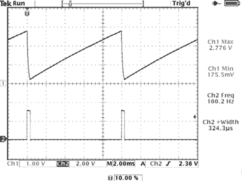
When VC = VTL, the comparator's output drops to zero, restores the initial state, and repeats the sequence. As Trace 1 in Figure 2 shows, the circuit behaves as a free-running oscillator in which the voltage across C5 ramps up and down between the Schmitt trigger's threshold voltages. Given that the discharge-time constant, τD, is much less than the charging-time constant, τC, the discharge time, tON, is considerably shorter than the integrating time, tX. As Trace 2 in Figure 2 shows, the comparator's output delivers a PPM signal having a relatively short pulse of approximately 320 µsec.
 |
|
| Figure 2. | Oscilloscope measurements of the VFC show voltage across capacitor C5 (upper trace) and comparator IC2’s output voltage, VOUT (lower trace), for a nominal input voltage of 12 V. |
Equations 5 and 6, respectively, describe the complete expressions for calculating the pulse widths of waveforms tX and tON:
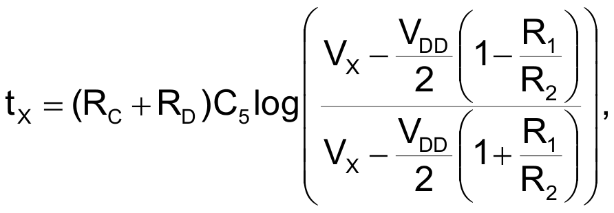 |
(5) |
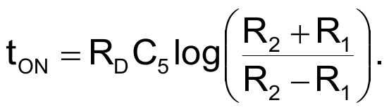 |
(6) |
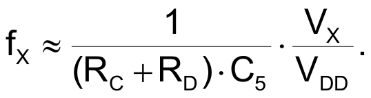
These formulas are useful for designing the VFC in Figure 1 but yield little insight into the circuit's global-transfer function. You can apply the following approximations to simplify the calculations: Because tX >> tON, the PPM output frequency is approximately fX ≈ 1/tX. In normal operation, VX reaches relatively high values when compared with the Schmitt trigger's threshold voltages, and you can linearize the charging law of capacitor C5 to a ramp having a constant slope (Equation 7).
 |
(7) |
According to Equation 4, the Schmitt trigger's high and low threshold voltages are, respectively, VTH ≈ VDD and VTL ≈ 0 V. Using these approximations, the PPM output frequency simplifies to:
 |
(8) |
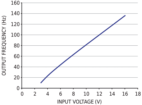
Equation 8 shows that the circuit in Figure 1 exhibits a voltage-to-frequency transfer function, as Figure 3 experimentally confirms. The VFC's power consumption is low; for example, at a dc voltage of 12 V, the VFC's current drain is about 36 µA.
 |
|
| Figure 3. | The measured transfer function of the VFC exhibits excellent linearity over a wide range of inductively coupled input voltages. |
