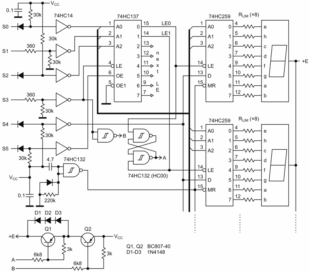
This design idea (Figure 1) shows how easily “new flesh can be added to the old bones” and how some new functions can be added to the simple LED display that was published earlier (Reference 1).
 |
|
| Figure 1. | Upgraded simple LED display that preserves the same interface but adds more functions. |
The design preserves the same interface, albeit some controls have additional functions.
The new features of the design are:
- Identification of the display by the host µP;
- Control of brightness (2 or more levels);
- A longer interface cable due to less sensitivity to ambient electric noise;
- Protection of the ICs against the loss of VCC;
- Reset display during power-on (all segments are On);
- Luminescence can be put out;
- Some add-on functions, which can be used for further modifications or for external applications;
- And, of course, PWM for the true connoisseurs.
If there are several devices sharing the same socket, the host µP can identify this display by reading the bits S5…S0 and comparing the result with the code 110101.
There are 2 levels of static brightness (albeit there may be more).
The level is selected by the sequence in which the digits of the display are programmed: from the digit which corresponds to LE0, to the digit which corresponds LE1, or the opposite sequence.
The selection is preserved by the RS-trigger which controls the BJT switch Q1 (BC807).
The sequence from LE1 to LE0 sets the output of the RS-trigger to A = 0 and the BJT Q1 is activated. This corresponds to full brightness.
The sequence from LE0 to LE1 sets the output of the RS-trigger to A = 1, so the BJT switch Q1 is off, and the LEDs receive a reduced current.
The same principle can be used to add more functions to the interface.
The algorithm of the interface:
- Initial/displaying state: S3 = 0, S5 = 1, all other pins are of no importance;
The steps required to change the data on the display are:
- Set a digit’s address: S2..S0 = address;
- S3 = positive strobe 0-1-0 to latch the address;
- Set a segment’s address on S2..S0;
- Set a value of D: S4 = 1 if the segment must be ON, S4 = 0 if OFF;
- S5 = negative strobe 1-0-1 to latch the value of D;
- Repeat from (3) for another segment, when all the segments are done, go to (1) while there are unattended digits.
- To turn the luminescence off: S3 = 1, S5 = 1
So, to get PWM you can simply play with S3 while holding S5 = 1.
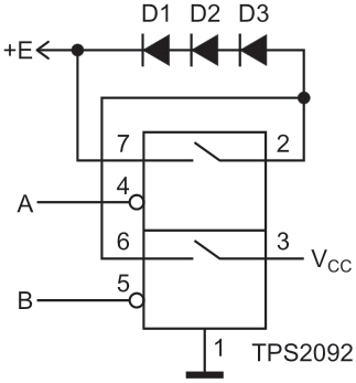
The power switch in Figure 2 is even simpler and consumes less power. It uses dual power-distribution switch TPS2092 instead of BJT switches. This circuit will also limit the current if an overload or short circuit are encountered.
 |
|
| Figure 2. | Power switch that is simpler and consumes less power than the BJT switches shown in Figure 1. |
Note:
- In this case you have to limit VCC to 5.5-V max;
- PWM would be somewhat restricted by 2.5-ms typical rise time of the switch.
References
- Demchenko, Peter. “An LED display adapted for DIY projects.“