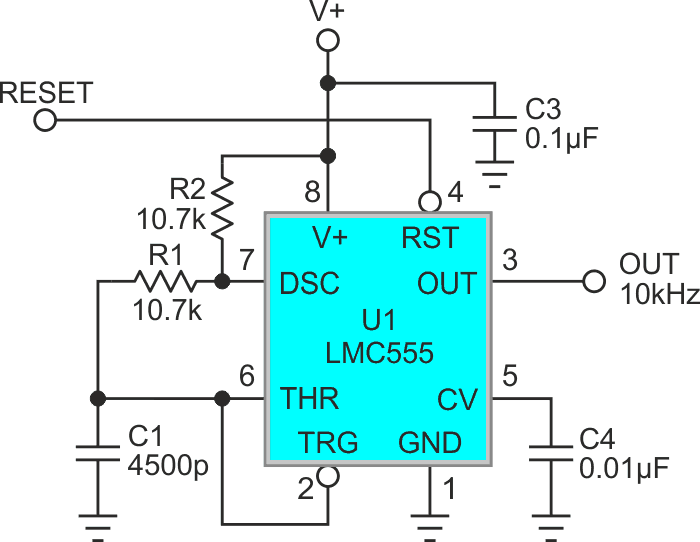
The classic and versatile 555 finds its way into many low to moderate frequency oscillator applications. Some of these require the ability to selectively gate oscillation on and off on demand and the 555’s RESET pin can conveniently be used for this purpose as shown in Figure 1.
 |
|
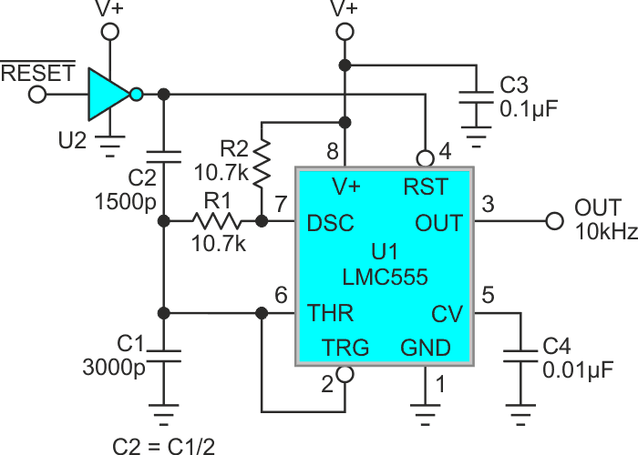
| Figure 1. | Typical gated (via RESET pin) 555 astable multivibrator. |
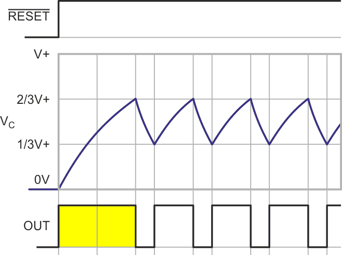
When asserted (logic level zero), RESET holds the output low and the frequency-setting RC in a known and accurately repeatable (discharged) state. But there’s a “gotcha” that occurs when RESET is returned to logic 1 and oscillation resumes. The problem is illustrated in Figure 2.
 |
|
| Figure 2. | Excessively long first pulse occurs on oscillation restart due to C1 complete discharge. |
The first pulse generated on restart is significantly longer than those that occur later. This is because during the oscillation-off interval, timing capacitor C1 is allowed to discharge completely to 0 V. This differs from the 1/3V+ “trigger” level that applies during steady-stage oscillation and results in a much longer ramp interval, which is problematic in some applications.
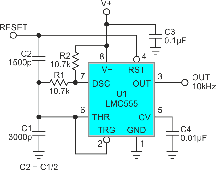
Happily, there’s a simple fix, illustrated in Figure 3.
 |
|
| Figure 3. | Added timing capacitor C2 immediately precharges C1 to V+/3 trigger level when RESET returns high normalizing the duration of the first oscillation cycle. |
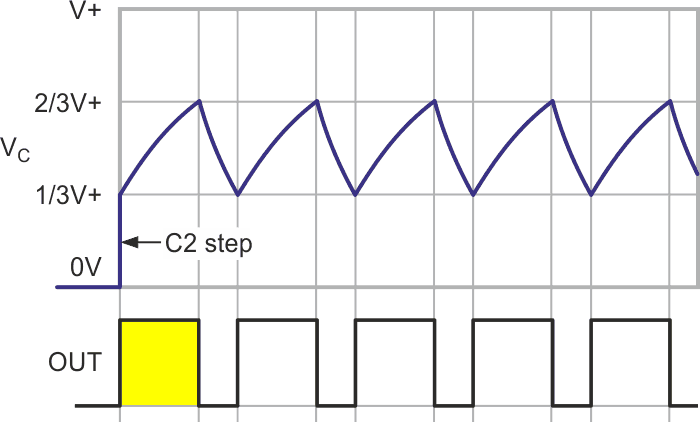
The original C1 timing capacitance is divided into two series/parallel connected capacitors, so that the new C1 = 2/3 of the original, and C2 = 1/3. The new oscillation start-up sequence is shown in Figure 4, note the slew to 1/3V+ on oscillation startup.
 |
|
| Figure 4. | C2 charge injection on oscillation startup equalizes pulse length. |
For this scheme to work accurately, the source of RESET must provide a full 0 to V+ step and present a low impedance compatible with generation of the timing ramp when at V+. If such a signal source doesn’t already exist, a buffer such as illustrated in Figure 5 may be necessary. A typical buffer choice would be something comparable to a 74HC04.
 |
|
| Figure 5. | A buffer may be necessary to provide a full voltage excursion RESET signal. |
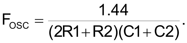
Oscillator design equations are unchanged from the usual 555 datasheet math, except that the timing capacitance used should be the sum C1 + C2.
Also necessary is that RESET be asserted and oscillation paused for a minimum of several R1(C1 + C2) time-constants (e.g., 5 or 6) between gates so that discharge of the timing capacitor will be accurately complete.
