I2C is a popular bidirectional serial communications bus having a clock and a data line. Both line’s drivers consist of an open drain ground-referenced N-channel MOSFET with a pullup resistor connected to a supply ranging from 1.8 V to 5 V. The pullup resistor must be small enough to meet certain timing requirements in the presence of significant bus capacitance, but large enough that the surprisingly weak active driver (specified to drop less than 0.4 V at 3 mA for standard mode and less than 0.6 V at 6 mA for fast mode speeds) current is not exceeded and that the logic low levels are met. Meeting both needs can be a challenge.
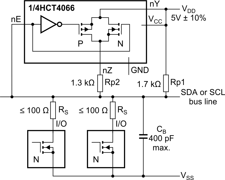
Figure 44 in section 7.24 of the “UM10204 I2C-bus specification and user manual“ (Ref, 1) presents a method of amelioration (Figure 1).
 |
|
| Figure 1. | Switched-pullup circuit where the analog switch is activated at high bus voltages only, paralleling an additional resistor with the standard pullup. |
An analog switch is activated at the higher bus voltages only, paralleling an additional resistor with the standard pullup. This reduces rise time without raising the driver’s achievable logic low level. But when the driver is activated, the amount of improvement is limited by the presence of the additional resistor at the higher voltages – too small an additional pullup, and the allowed driver current will be exceeded, and the required logic low level will not be met. A better approach would be to connect the additional resistor only when the signal is rising, that is, when the driver is off. The driver would then not be fighting the additional pullup, which accordingly could be made extremely small. This is the approach taken with the following circuit.
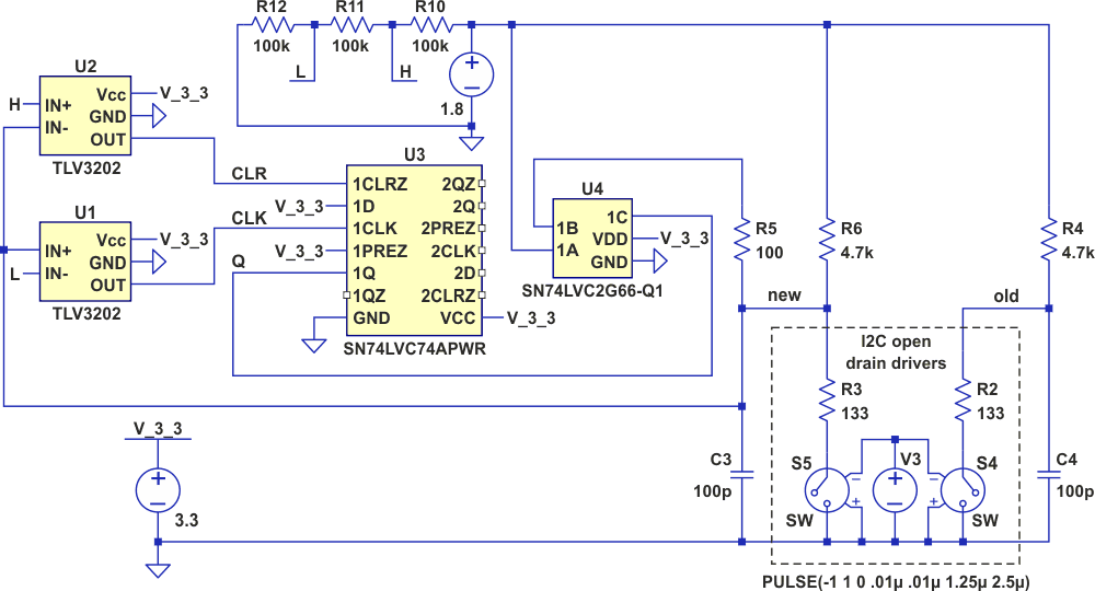
In Figure 2, comparators U1 and U2 are set to switch at the logic low and high thresholds of a typical 1.8 V I2C bus.
 |
|
| Figure 2. | A schematic of simulated I2C drivers, pullup resistors and bus capacitances, without (old) and with (new) connection to the autonomous non-linear pullup circuit. |
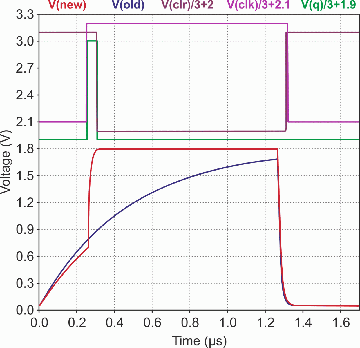
When the driver turns off and releases the signal “new” from a logic low, that signal rises through the low threshold. There is an acceptable propagation-delayed positive output transition of U1 which clocks the 1Q output of D flipflop U3 to a logic high. This activates U4, switching R5 in parallel with the standard pullup R6 and greatly reducing rise time. As the signal rises through the logic high level, the output of U2 transitions to a logic low, clearing the 1Q output of U3, deactivating U4 and disconnecting R5. (In this instance, the propagation delay is welcome. U2’s delay allows the signal time to reach 1.8 V, courtesy of the additional pullup.) The circuit is now ready for the driver’s next activation, which will happen without it having to fight R5. Until activation, the circuit draws negligible current. Figure 3 shows the reduced rise time of the “new” circuit in comparison to that of the “old”, both having the same bus capacitance and same standard pullup. 100 pF is only 25% of the maximum specified value for I2C operation.
 |
|
| Figure 3. | A comparison of the performances of standard (old) and an enhanced (new) I2C bus signals. The signals CLR, CLK, and Q swing between ground and +3.3 V are shown scaled for clarity purposes. |
Although 1.8 V is a popular bus voltage (especially for smart battery IC’s), I was unable to find suitably fast, adequately low supply current comparators which can be powered from this voltage. Fortunately, 3.3 V is generally available in products with 1.8 V buses, and an analog switch serves admirably to bridge the gap between the two supplies. If the bus runs at 3.3 V, the analog switch can be replaced with a PNP transistor whose emitter is connected to the bus’s supply, and its base driven through a 3.3k resistor. In the unlikely event of a 5 V bus, 5 V can be connected to the PNP’s emitter, but a 5 V-supply-capable D flip-flop will need to be found to replace U3.
