LVDS Transmitters, Receivers Deliver 400 Mbps of Performance in Extreme Environments
National Semiconductor Corporation introduced five new extended temperature single and dual transmitters and receivers to the company’s industry-leading portfolio of low-voltage differential signaling (LVDS) products. The general-purpose LVDS physical layer devices (PHYs) are optimized for driving signals through cable harnesses in systems operating in harsh, high-temperature environments, such as automotive, industrial and military applications.
In a typical application, the LVDS PHYs improve signal integrity by translating the single-ended control and data signals from sensors into LVDS signals for transmitting to the digital processor, typically an FPGA or ASIC. In automotive or industrial systems where electrical noise is often unavoidable, LVDS is the best signaling technology choice because of its superior noise immunity and error-free performance.
Technical Features of the Extended Temperature LVDS PHYs
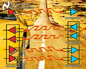
The five new extended temperature single and dual transmitters and receivers support the differential LVDS interface standard from -40 degrees C to +125 degrees C. The DS90LV011AH transmitter, DS90LT012AH receiver, DS90LV027AH dual transmitter, DS90LV028AH dual receiver and DS90LV049H integrated dual transceiver functions use the LVDS analog interface to provide a high-performance signal path that transfers digital information. In addition, the DS90LT012AH features an integrated LVDS input termination to save board space. The DS90LV027AH and DS90LV028AH feature a flow-through pin-out to simplify board layout.
All of the LVDS PHYs are offered in extremely small packages to minimize board space. The DS90LV011AH and DS90LT012AH are packaged in a 5-pin SOT-23. The DS90LT012AH is also available as a bare die. The DS90LV027AH and DS90LV028AH are packaged in an 8-pin SOIC and the DS90LV049H is packaged in a 16-pin TSSOP. Lead-free package options are also available.
