Holtek is delighted to announce the release of its new 8 bit TinyPowerTM A/D with LCD type Flash MCU series. This device series includes the full feature range of the Enhanced Flash MCUs while also incorporating Holtek’s unique TinyPowerTM technology. With its ultra low power consumption, fast wake-up, multiple clock sources and range of operating modes that greatly reduces power requirements, this new device range is positioned to meet the demands of today’s environmentally conscious products. The device range is suitable for applications such as household appliances, instrumentation products, industrial control, health products, exercise equipment etc.

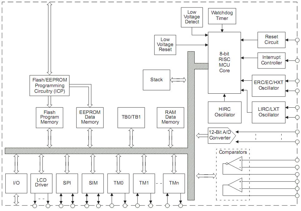
The HT67Fxx series is composed of four MCU devices (HT67F30, HT67F40, HT67F50 and HT67F60) encompassing a full range of multiple functions. These include a core with 2K~12K word of Flash Program Memory, 128~640 bytes of Data Memory, 64~256 bytes of Data EEPROM and 4~12 stack levels. Regarding peripheral functions, all devices contain an internal R-type and power-efficient C-type LCD driver to support applications with display requirements. The internal 12-bit high speed analog to digital converter is on hand to measure external environmental signals from sensors such as temperature, humidity etc. An internal comparator and two independent SPI and SPI/I2C interfaces are also included while the whole series use Holtek’s new Timer Modules offering five different timer operating modes, namely Input Capture, Compare, Timer/Event, Single Pulse Output and PWM. These features combine to offer a device series that can implement a full MCU system with a minimum of external components.
- CPU Features
- Operating Voltage:
- fSYS= 4MHz: 2.2V~5.5V
- fSYS= 8MHz: 2.4V~5.5V
- fSYS= 12MHz: 2.7V~5.5V
- fSYS= 20MHz: 4.5V~5.5V
- Up to 0.2µs instruction cycle with 20MHz system clock at VDD=5V
- Power down and wake-up functions to reduce power consumption
- Six oscillators:
- External Crystal - HXT
- External 32.768kHz Crystal - LXT
- External RC - ERC
- External Clock - EC
- Internal RC - HIRC
- Internal 32kHz RC - LIRC
- Multi-mode operation: NORMAL, SLOW, IDLE and SLEEP
- Fully integrated internal 4MHz, 8MHz and 12MHz oscillator requires no external components
- All instructions executed in one or two instruction cycles
- Table read instructions
- 63 powerful instructions
- Up to 12-level subroutine nesting
- Bit manipulation instruction
- Operating Voltage:
- Peripheral Features
- Flash Program Memory: 2Kx15 ~ 12Kx16
- RAM Data Memory: 128x8 ~ 640x8
- EEPROM Memory: 64x8 ~ 256x8
- Watchdog Timer function
- Up to 64 bidirectional I/O lines
- LCD driver function
- Multiple pin-shared external interrupts
- Multiple Timer Module for time measure, input capture, compare match output, PWM output or single pulse output function
- Serial Interfaces Module with Dual SPI and I2C interfaces
- Single Serial SPI Interface
- Dual Comparator functions
- Dual Time-Base functions for generation of fixed time interrupt signals
- Multi-channel 12-bit resolution A/D converter
- Low voltage reset function
- Low voltage detect function
- Wide range of available package types
HT67Fxx Block Diagram
Holtek also fully supports these devices with its comprehensive hardware and software development tools. Known s the HT-IDE3000, these development tools provide features such as real time emulation, memory and register access, hardware breakpoints complete with logical setups, full trace analysis etc. This range of development tools ensure that designers have all the resources at hand to provide for rapid and efficient design and debug of their microcontroller based new product applications.

