Analog Devices
Circuit Note CN-0038
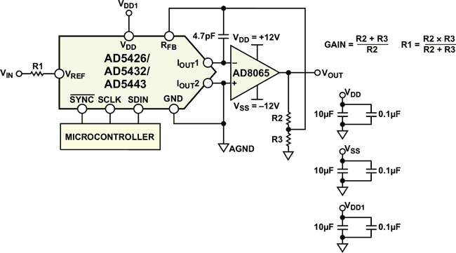
Circuit Function and Benefits
This circuit provides a programmable gain function using a multiplying DAC and an operational amplifier (op amp). The maximum gain value and the temperature coefficient are set by the external resistors and the resolution of the programmable gain is set by the resolution of the DAC.
 |
||
| Figure 1. | Programmable Gain Circuit Using a Current Output DAC (Simplified Schematic). | |
Circuit Description
The circuit shown in Figure 1 is the recommended method for increasing the gain of the circuit. R1, R2, and R3 should all have similar temperature coefficients, but they need not match the temperature coefficients of the DAC. This approach is recommended in circuits where gains of greater than 1 are required. The gain is
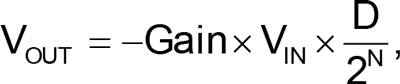
where D is the digital word loaded to the DAC and N is the number of bits: D = 0 to 255 (8-bit AD5426); D = 0 to 1023 (10-bit AD5432); and D = 0 to 4095 (12-bit AD5443). The key benefit of this circuit is its ability to overcome gain TC errors using resistor matching. The TC of the external resistors need to match each other, but do not need to match that of the DAC internal ladder resistance. Resistor R1 is required because R1 plus the input impedance of the DAC must equal the total feedback resistance, which is RFB plus R2||R3. The input impedance of the DAC is RFB, so
R1 + RFB = RFB + R2||R3,
R1 = R2||R3.
The values of R1 and R2 must be chosen so that the output voltage does not exceed the output range of the operational amplifier for the given supply voltage. Also, note that the bias current of the operational amplifier is multiplied by the total feedback resistance (RFB + R2||R3) to give an associated offset. Therefore, the values of R1 and R2 cannot be too large or they will have a significant effect on the overall output offset voltage.
The input offset voltage of an op amp is multiplied by the variable gain (due to the code-dependent output resistance of the DAC) of the circuit. A change in this noise gain between two adjacent digital fractions produces a step change in the output voltage due to the amplifier’s input offset voltage. This output voltage change is superimposed on the desired change in output between the two codes and gives rise to a differential linearity error that, if large enough, could cause the DAC to be nonmonotonic. The AD8065 benefits from both a low input offset voltage and low bias currents to overcome this issue.
Common Variations
The OP1177 is another excellent op amp candidate for the I-V conversion circuit. It also provides a low offset voltage and ultralow bias current. For the selection of the reference, the input voltage is restricted by the rail-to-rail voltage of the operational amplifier selected and also the gain set up by resistors R2 and R3.