Using a shift register with parallel output is a common way to design a pulse generator with N inputs and pulsed outputs having a width of T/N. To keep the output pulses consecutive, you can use feedback from the last output to the first input. At power-on, such a circuit can have a random combination of logic zeros and ones, forming an undesired data content of the shift register. To avoid circulating undesired states and to enter a proper sequence, you need a special feedback.
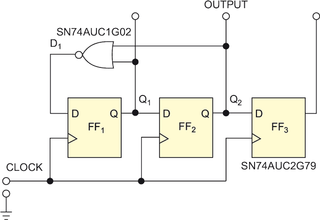
The circuit in Figure 1 is a three-stage shift register that uses D-type flip-flops. It has three outputs, Q1, Q2, and Q3, each of which produces a periodic pulse having a width of TREP/3. TREP = 3TCLK is the period at which the sequence repeats at any of the three outputs. A two-input NOR gate creates the feedback. The gate’s D1 output connects to the D input of flip-flop FF1, and its inputs connect to Q1 and Q2. A logic-one bit at D1 means that, at the nearest low-to-high transition of the clock, this signal will place a logic one at output Q1.
 |
||
| Figure 1. | This one-of-three pulse generator uses three ICs, yet it avoids false logic states. | |
You can interpret this feedback in words by writing a logic zero into FF1 at the nearest low-to-high transition of the clock signal, if at least one of the Q1 or Q2 outputs has a logic-one state. You write a logic one into FF1 if both the Q1 and the Q2 outputs are at logic zero. This feedback adds a self-correcting feature, which is illustrated by the assumption that the initial state of the circuit is intentionally undesired.
Using this result, the following sequences illustrate state correction, in which the logical states in the bit triads correspond left to right to Q1, Q2, and Q3:
111→011→001→100→010→001
000→100→010→001
From this example, you can see that erroneous state 111 self-corrects within two periods of the clock. For the undesired 000 state, the proper cycling enters at the nearest low-to-high transition of the clock signal.
 |
||
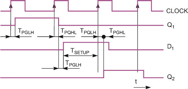
| Figure 2. | The circuit generates glitch-free logic waveforms that are successive in time and have accurate duty cycles of 33.3%. |
|
You can determine the upper limit of the clock frequency from an assumption of the gate output, which changes after a low-to-high transition of the clock. This condition must be ready with a setup time, TSETUP, the next time the clock transitions from low to high (Figure 2). Thus,
TCLKMIN = TPQHL + TPGLH + TSETUP,
where TPQHL and TPGLH are signal-propagation delays of the flip-flop and the gate, respectively, at the respective output-level transition. By using the worst-case values of propagation delays from the devices’ data sheets, you get a minimum clock period of 4.4 nsec for a supply voltage of 1.8 V and a minimum clock period of 3.5 nsec for a supply voltage of 2.5 V. As the 3.5-nsec value gives a clock frequency higher than the guaranteed toggle frequency for the flip-flop, you should accept the maximum clock frequency at 275 MHz for a supply voltage of 2.5 V. For a supply voltage of 1.8 V, the maximum clock frequency should be 227 MHz. The maximum repetition rate of signals at Q1, Q2, and Q3 outputs is the maximum clock frequency divided by three, or 75.6 MHz.