Robert F. Coughlin
Electronic Design
Adding “intelligence” to measurement systems has become commonplace because 8-bit microcontrollers are inexpensive and widely available, and they can be programmed in many of today’s popular higher-level languages (e.g., C and Basic). Often, the main challenge is signal-conditioning the sensor’s output into a signal-ended voltage that can fully exploit the input span of the microcontroller’s analog-to-digital converter (ADC).
By using basic math and a systematic approach, you can easily identify and design the needed hardware. This design technique is general enough to apply to all linear sensors.
 |
|
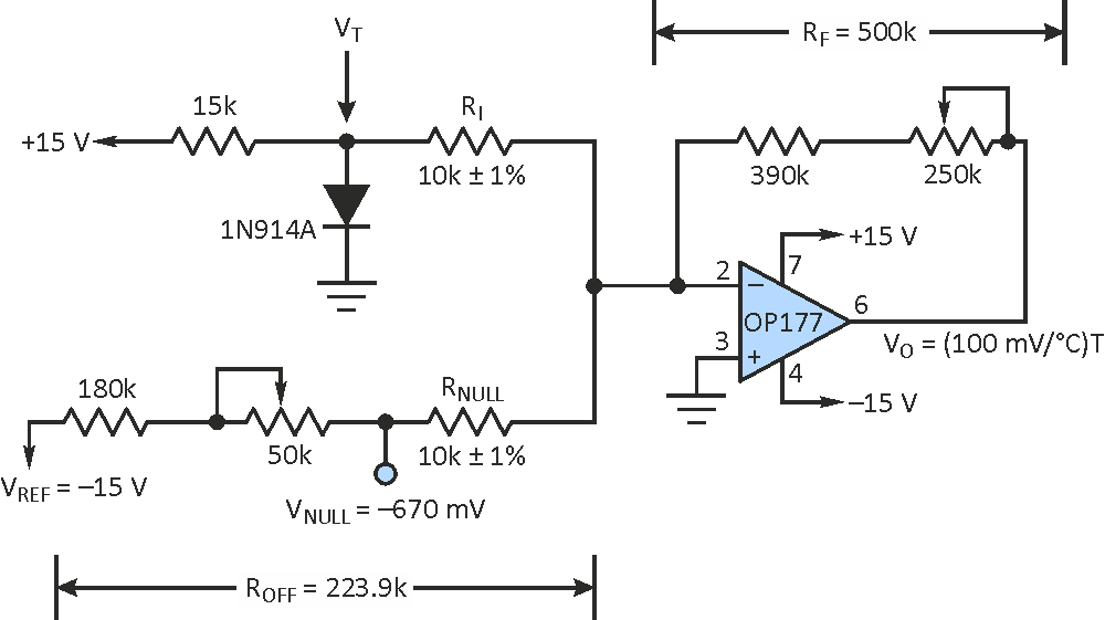
| Figure 1. | Several simple equations make it easy to design this signal-conditioning circuit for interfacing a temperature sensor with a microcontroller. |
Consider a design that must convert temperature ranging from 0 °C to 50 °C into a 0- to 5-V signal – a common input span for 8-bit ADCs. The equation to describe this linear sensor system is:
 |
(1) |
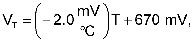
If we select a low-cost 1N914A silicon diode as the temperature sensor, we can characterize its linear performance with a sensor equation that’s typical of this type of semiconductor-based temperature detector:
 |
(2) |
where VT is the diode’s temperature-derived signal. By solving Equation 2 for the temperature, T, and substituting into the system equation, Equation 1, we get the signal-conditioning circuit’s design equation, which describes the electronics needed to properly interface the sensor to the microcontroller’s ADC input:
 |
(3) |
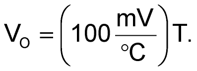
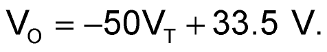
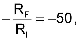
Equation 3 indicates that the signal-conditioning circuit must amplify VT by a gain of –50 and offset this voltage by 33.5 V. The circuit depicted in the Figure 1 can implement this design equation because its performance equation is:
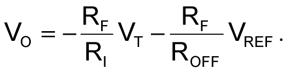 |
(4) |
Comparing the design equation (Equation 3) and performance equation (Equation 4) terms simplifies component selection. The signal path of the inverting adder circuit is set by making the gain terms’ resistance ratio,
and the offset term,
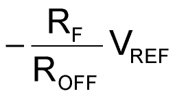
set to the needed 33.5 V.
Making RNULL = RI enables you to calibrate the zero point of the circuit at any temperature. First, measure VNULL and adjust the 50-kW ROFF potentiometer for a voltage of –670 mV, which is the sensor’s output at 0 °C. Then, with the sensor stable at a known temperature (for example, 24 °C), adjust the –50-kW RF potentiometer to make the output voltage of the operational amplifier conform to the system equation:
VO (@ 24 °C) = (100 mV/°C)×(24 °C) = 2.40 V.