George Qian, Linear Technology
Design Note 559
Introduction
In traditional isolated high voltage flyback converters, tight regulation is achieved using opto-couplers to transfer regulation information from the secondary-side reference circuitry to the primary side. The problem is that opto-couplers add significant complexity to isolated designs: there is propagation delay, aging, and gain variation, all of which complicate power supply loop compensation and can reduce reliability. Moreover, during start-up, either a bleeder resistor or high voltage start-up circuit is required to initially power up the IC. Unless an additional high voltage MOSFET is added to the start-up components, the bleeder resistor is a source of unwelcome power loss.
The LT8315 is a high voltage flyback converter with an integrated 630 V/300 mA switch. The LT8315 eliminates the need for an opto-coupler, complicated secondary-side reference circuitry, additional start-up components, and an external high voltage MOSFET.
Performance and Simplicity
The LT8315 integrates a 630 V MOSFET and control circuitry inside a thermally enhanced 20-pin TSSOP package with four pins removed for high voltage spacing. By sampling the isolated output voltage from the third winding, no opto-coupler is required for regulation. The output voltage is programmed with two external resistors and a third optional temperature compensation resistor. Boundary mode operation helps to achieve excellent load regulation. Because the output voltage is sensed when the secondary current is almost zero, no external load compensating resistors and capacitors are needed. As a result, the LT8315 solution has a low component count, greatly simplifying the design of an isolated flyback converter.
 |
||
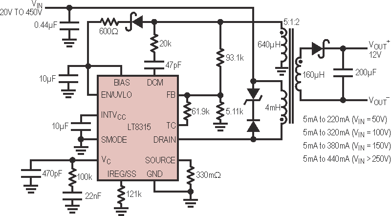
| Figure 1. | A Complete 12 V Isolated Flyback Converter for a Wide Input from 20 V to 450 V. | |
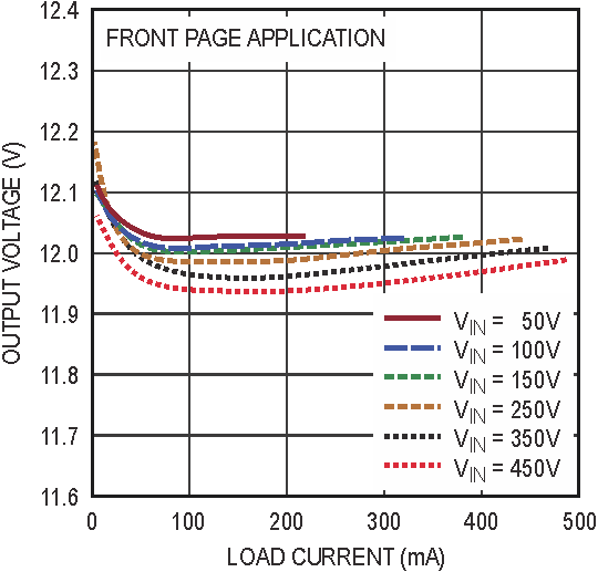
Figure 1 shows the complete schematic of a flyback converter with a wide input range from 20 V to 450 V. It has a 12 V output and maintains tight regulation with a load current from 5 mA to over 440 mA. The output current capability increases with input voltage, the output current could reach 440 mA when the input voltage exceeds 250 V. This flyback converter has 85% peak efficiency. Even with no opto-coupler, load and line regulation remain tight, as shown in Figure 2.
 |
||
| Figure 2. | Load and Line Regulation of the Flyback Converter in Figure 1. | |
Internal Depletion MOSFET for Start-Up
The LT8315 features an internal depletion mode MOSFET, which has a negative threshold voltage and is normally on. At start-up, this MOSFET charges the INTVCC capacitor to 12 V so that the LT8315 has power to begin switching. As a result, there is no need for an external bleeder resistor or other start-up components. Once INTVCC is charged, the depletion mode MOSFET turns off to reduce power loss.
Low Quiescent Current
The LT8315 typically requires a small preload at the output, which reflects back to the input as quiescent current. As the load gets very light, the LT8315 reduces the switching frequency while keeping the minimum current limit in order to reduce current while properly sampling the output voltage. The typical minimum switching frequency is about 3.5 kHz. When the standby mode is enabled, the minimum frequency is further reduced to 220 Hz, which is a 16× reduction for ultralow quiescent current.
In standby mode, the LT8315’s preload is usually less than 0.1% of full output power, the quiescent current is lower than 100 μA – important for applications requiring high efficiency in always-on systems.
Nonisolated Buck Converter
The LT8315’s high voltage input capability is easily applied in nonisolated solutions. Nonisolated converters do not require the transformer of an isolated converter, instead adopting a relatively inexpensive off-the-shelf inductor as the magnetizing component.
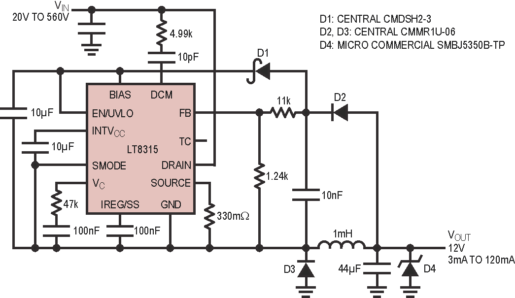
For a nonisolated buck application, the LT8315’s ground pin is connected to the switch node of the buck topology, which is a varying voltage. The unique sensing scheme of LT8315 sees the output voltage only when the switch node is connected to ground, which leads to a simple buck schematic, as shown in Figure 3. The diode, D2 and two resistors at the FB pin form the feedback path.
 |
||
| Figure 3. | Schematic of a Nonisolated Buck Converter: 20 V to 560 V Input to 12 V at 120 mA. |
|
Figure 3 shows the schematic of a nonisolated buck converter, which converts an extremely wide-ranging input of 20 V to 560 V, to a regulated 12 V output. This circuit can achieve efficiency as high as 85%.
Conclusion
The LT8315 operates at a wide input voltage range of 18 V to 560 V, delivering up to 15 W of isolated output power. It requires no opto-coupler, and includes rich features such as low ripple Burst Mode® operation, soft-start, programmable current limit, undervoltage lockout, temperature compensation, and low quiescent current.
The high level of integration simplifies the design of low component count, high efficiency solutions in a wide variety of applications: from battery powered systems to automotive, industrial, medical, telecommunications power supplies and isolated auxiliary/ housekeeping power supplies.