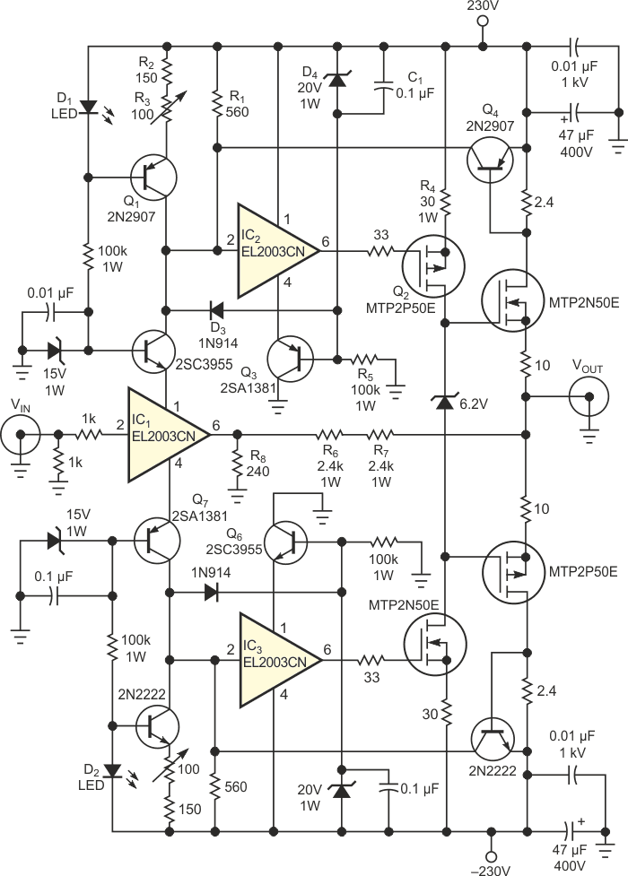
The circuit in Figure 1 powers a microparticle and nanoparticle ion trap through a 1-to-5-turns-ratio, high-voltage transformer. It also works successfully as a driver for a piezo-tube scanner and in a near-field scanning optical microscope. The circuit is robust and works with supplies ranging from ±50 to ±230 V. The measured parameters at ±230 V supply voltage are gain of 26-dB from dc to –3-dB point at 7 MHz; output swing of ±200 V, rise and fall times of 70 nsec for an output step of 350 V, slew rate of 4100 V/µsec, and supply current of 56 mA.
 |
||
| Figure 1. | This high-voltage, current-feedback amplifier slews at 4100 V/µsec. | |
The red LEDs, D1 and D2, in Figure 1 provide a 1.8 V drop; the LEDs are more rugged than precision IC voltage references. The current supply for IC1 comes from R1 and the source comprising D1, R2, R3, and Q1. R3’s trimmed value is such that Q2’s quiescent current is approximately 15 mA. You can determine this current by measuring the voltage drop across R4. The same adjustment also controls the output-voltage offset. IC2 is a unity-gain, high-current driver for Q2. D3 prevents IC2’s input from going more negative than its negative supply. Q3, D4, C1, and R5 provide the negative bias for IC2. Q4 is an output-current limiting switch. Q4 starts to turn on at IOUT = 290 mA. You can replace the bipolar transistors 2SC3955 (npn, Q2 and Q6) and 2SA1381 (pnp, Q3 and Q7) by equivalents as long as they have the following minimum specs: VCEO ≥ 250 V; IC ≥ 100 mA, and fT ≥ 100 MHz.
 |
||
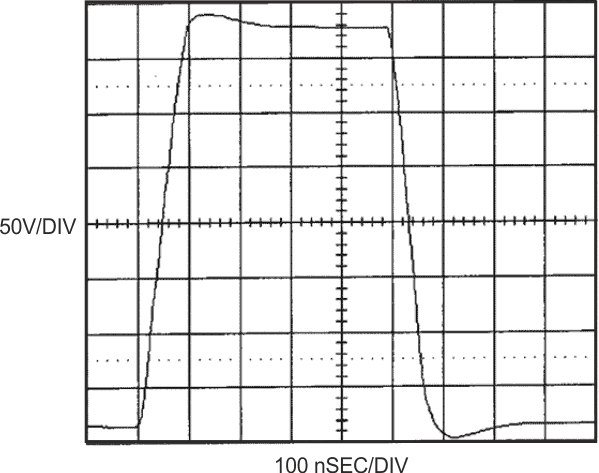
| Figure 2. | The circuit has a clean square-wave response with minimal over-shoot and no ringing. |
|
You should mount all the power transistors in individual finned heat sinks with an overhead 3-in. fan for cooling. The pc-board layout is not critical and needs no ground plane. However, you must use single-point grounding to minimize ringing. For the component values shown, the circuit is very stable and needs no compensation capacitors. Figure 2 shows a large-signal response for a ±9 V, 1-MHz square-wave input. This circuit has a fixed gain of 20. For higher gains, you can increase the values of R6 and R7. For lower values, it is better to insert an attenuator at the input, because smaller values of R6 and R7 may result in excessive dissipation. Do not change the value of R8, because it is optimized for speed. Be cautious when measuring and using this circuit, because it harbors lethal voltages.
