Introduction
High voltage buck DC/DC controllers such as the LTC3890 (dual output) and LTC3891 (single output) are popular in automotive applications due to their extremely wide 4 V to 60 V input voltage range, eliminating the need for a snubber and voltage suppression circuitry. These controllers are also well suited for 48 V telecom applications where no galvanic isolation is required.
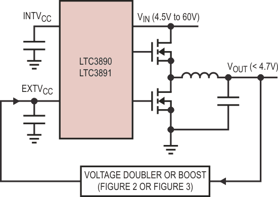
In a typical application for these controllers, the IC’s supply voltage (INTVCC) is provided by the on-chip LDO. This LDO produces 5 V from input voltages up to 60 V to bias control circuitry and provide power FET gate drive. Although simple, this built-in biasing scheme can be inefficient. Power losses can be significant in applications where the input voltage is consistently high, such as in 48 V telecom applications. Reducing the power losses in the bias conversion can increase efficiency and also reduce the controller case operating temperature.
Employing EXTVCC to improve efficiency
One of the attractive features of the LTC3890 and LTC3891 controllers is the external power input (EXTVCC). This is a second on-chip LDO, which can be used to bias the chip. When the input voltage is consistently high, it is more efficient to produce the biasing voltage by stepping down the converter’s output voltage, which is fed into EXTVCC, rather than generating 5 V INTVCC from the high input voltage.
Figure 1 shows a block diagram for this scheme. The output can be directly connected to the EXTVCC pin of the chip as long as the output voltage is above 4.7 V. However, extra circuitry (described in the following section) is required for outputs below 4.7 V.
 |
|
| Figure 1. | Block diagram showing external bias. |
Voltage doubler for output voltages below 4.7 V
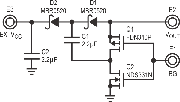
When the controller’s output is below 4.7 V, it must be stepped up to allow the built-in LDO to work. A simple voltage doubler solves this problem as long as the output is higher than 2.5 V. Below 2.5 V output, a multivibrator-based circuit can be used.
Figure 2 shows a simple, low cost solution for output voltages between 2.5 V and 4.7 V. This is a voltage doubler scheme based on small P-channel and N-channel MOSFETs, Q1 and Q2. The gates of these transistors are controlled by the bottom gate driver, BG of the controller. When BG is high, Q2 is on, Q1 is off and capacitor C1 charges from output voltage VOUT through D1. When BG is low, Q2 is off, Q1 is on and capacitor C1 delivers a voltage close to 2•VOUT to EXTVCC.
 |
|
| Figure 2. | Voltage doubler allows external bias from VOUT in the range of 2.5 V to 4.7 V. |
 |
|
| Figure 3. | Boost controlled by astable multivibrator is used for VOUT lower than 2.5 V. |
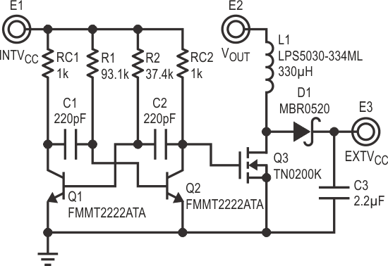
Figure 3 shows a solution for voltages below 2.5 V. The circuit consists of an astable multivibrator based on transistors Q1 and Q2, and a boost based on N-channel Q3 and inductor L1. Q1 and Q2 are biased from INTVCC and output voltage VOUT is stepped up to 5 V, which feeds EXTVCC. The multivibrator frequency, f, is set at 50 kHz to minimize the EMI signature. The pulse width is defined by the ratio of resistors R1 and R2, as per the following expressions:
Conclusion
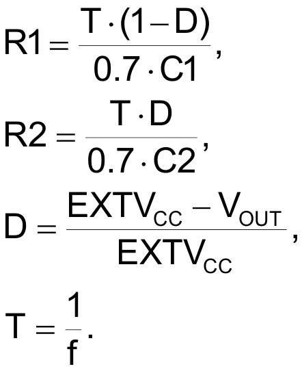
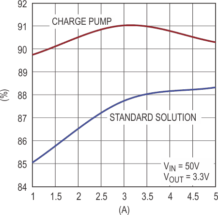
The efficiency of high input voltage DC/DC controllers can be significantly improved by using the controller’s output voltage to power the IC, instead of allowing the internal LDO to produce the bias voltage. For input voltages above 30 V, efficiency improvements of 2% to 3% are realized when a voltage doubler circuit is used for a 3.3 V at 5 A output (see Figure 4). Similar efficiency improvements are shown for a 1.8 V at 7 A converter with a multivibrator-based circuit.
 |
|
| Figure 4. | LTC3890/LTC3891 efficiency improvement. |
