Hubert Hagadorn
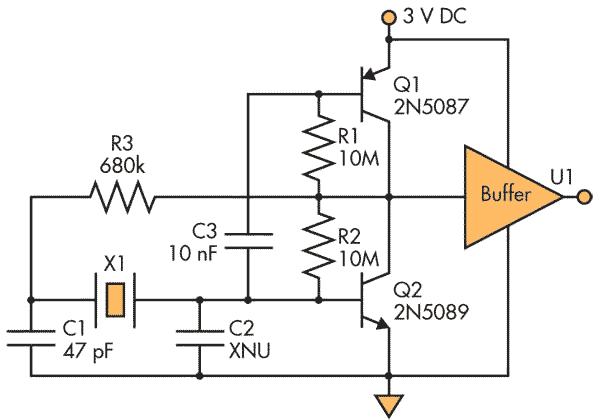
The Pierce-type resonant crystal oscillator in Figure 1 was designed to run off two series-connected 1.5-V batteries and reliably start at a supply voltage as low as 2.4 V. Tests had previously indicated that Pierce crystal oscillators using standard CD4000 inverters could not reliably start at such a low supply voltage, although once started they could operate at lower voltages.
 |
|
| Fig 1. | This Pierce-series resonant oscillator can reliably start at supply voltages as low as 2.4 V. It also draws very low current, ensuring long battery life. |
The low starting voltage was originally designed to allow a minimum battery life of one year in a particular clock design. The circuit shown was patented (No. 5,220,291), but the patent has expired.
The oscillator features a common-collector output drive having a rail-to-rail output, and it may be directly connected to digital CMOS logic. Most importantly, for long battery life, a very low operating current was required, so the output transistors were selected for their relatively high gain at low currents (20 µA). The crystal is a standard 32.768-kHz watch crystal (which divides down exactly to 1 Hz), having a frequency tolerance of ±20 ppm.
R1 and R2 bias transistors Q1 and Q2 at the supply mid-point. The oscillator’s output (at the collector connection) is connected to R3, which together with C1, X1, and C2 comprise a phase-shifting network. The output of this network is applied to the bases of Q1 and Q2, completing a regenerative loop.
C2 is not required but is included in the event that it may be desired in other circumstances. The loop has 360° of phase shift at the oscillating frequency. The oscillator output is also connected to buffer U1, which squares up the oscillator signal. A suitable buffer is a CD4000 series IC, such as an inverter, or a NAND or NOR wired as an inverter.
For a supply voltage of 3 V, the measured unloaded oscillator current was 1.4 µA (with the oscillator not connected to U1, a CD4011B NAND), the loaded oscillator current was 1.8 µA, and the combined oscillator and U1 currents were 3 µA.
 |
|
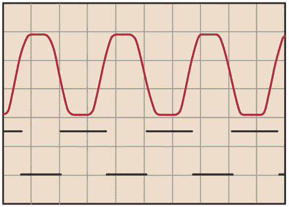
| Fig 2. | An oscilloscope photo shows the circuit’s 32.768-kHz signals (at 10 µs/cm): the oscillator’s output at 1 V/cm (top) and the buffer’s output at 2 V/cm (bottom). |
Figure 2 shows oscilloscope photos of the oscillator and U1 outputs. Note that directly connecting the oscillator output to high-speed CMOS circuitry will result in considerably greater supply currents owing to rise time considerations of the oscillator output and higher transition currents for high-speed CMOS. Thus, the CD4000 series buffer or a suitable alternative is advised.
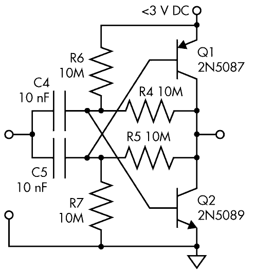
Also, Figure 3 shows an alternative biasing arrangement that allows operation at lower supply voltages. For the circuit in Figure 1, the supply voltage must be greater than the sum of the two base-emitter voltages. For the arrangement in Figure 3, the startup supply voltage is less than 2 V at 32.768 kHz. Interestingly, oscillations were observed for supply voltages as low as 0.65 V, with supply currents less than 1 µA.
 |
|
| Fig 3. | Designers can chose an alternative biasing arrangement that reduces the required startup voltage even lower—to less than 2 V. |
Some brief tests have indicated this oscillator may prove useful at much higher frequencies as well. At 30 MHz, a crystal operated at its third overtone with no difficulty. Q1, Q2, and C3 were unchanged; R1 and R2 were 330 kΩ, and R3 a short. C1 and C2 were not precisely determined, but were 1- to 40-pf variable capacitors that were adjusted to achieve minimum oscillator current. For a supply voltage of 3 V, an unloaded oscillator current of about 400 µA was measured.
