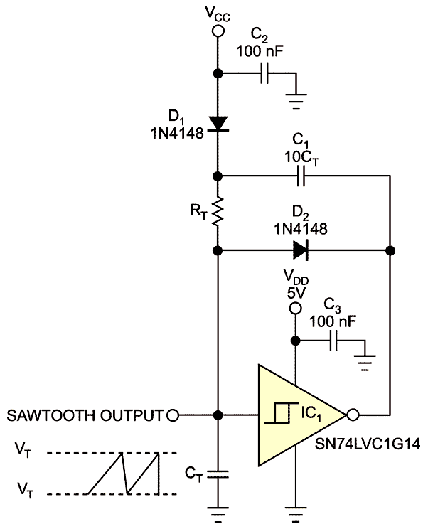
Pulse-width-modulation signal-generator circuits often use an analog sawtooth-oscillator function, but it also can be useful in other applications. The inexpensive sawtooth generator in Figure 1 suits use in low-power applications operating at frequencies as high as 10 MHz and beyond and those in which ramp linearity and frequency accuracy are not prominent concerns.
 |
|
|
Figure 1. |
You can use the CT ramp’s charge and fast discharge to produce a sawtooth. The upper and lower trippoint voltages of the Schmitt trigger limit the sawtooth. See text for the values of VCC, CT, and RT. |
The circuit employs a single Schmitt-trigger inverter, which acts as a modified astable multivibrator. The output waveform is the voltage across timing capacitor CT, which ramps between the lower and the upper threshold voltages of the inverter. Charging the RTCT network at constant voltage causes the ramp, so its response is exponential, approximately linear only for the initial part of the exponential rise.
A simple trick to improve ramp linearity is to charge the RTCT network with a higher-voltage source. Capacitor C1, which has a value that is at least 10 times greater than that of CT, acts as a charge pump. When the gate output is low during the falling edge of the sawtooth, capacitor C1 quickly charges through diode D1 to VCC minus the forward voltage of D1. Meanwhile, capacitor CT discharges quickly through diode D2.
When the falling CT voltage reaches the Schmitt trigger’s lower trip point, VT−, the gate output returns high. The charge on C1 drives the cathode of D1 to the sum of the voltage of capacitor C1 and the gate’s high output voltage. D1 becomes reverse-biased, and the RTCT network begins to charge to the voltage on C1, along with the gate’s high output voltage. When CT reaches the Schmitt trigger’s upper trip point, VT+, the gate’s output returns low, and the cycle repeats.
Ramp linearity is proportional to the sum of the VCC and VDD supply voltages. Because VDD is fixed at 5V, you can improve ramp linearity if VCC can assume a value higher than that of the inverter. You can estimate the ramp’s nonlinearity error using the following equation:

where ENL% is the percentage of nonlinearity error, MI is the initial slope of the ramp, and MF is the final slope of the ramp, and

where VF is the forward-voltage drop across D1.
The RTCT time constant sets the frequency, FO, of the sawtooth signal. You can estimate the frequency by applying a simple model to the circuit, which neglects the discharge time of CT and any discharge of CT, yielding the following equation:

where K is a constant, which the following equation defines:

By simulating the circuit with CT=100 pF and RT=2.2 kΩ, which agree with the values that the equations theoretically calculated, you can obtain ramp-nonlinearity errors of 28% with both VCC and VDD equal to 5V, 18% with VCC of 10V and VDD of 5V, and 14% with VCC of 15V and VDD of 5V.
The breadboarded circuit has VDD=VCC=5V, CT=100 pF, and RT=2.2 kΩ. IC1 is a standard dual-in-line, eight-pin 74HC14, which has a maximum propagation delay of 15 nsec versus 4.4 nsec for the SN74LVC1G14 inverter with a VDD of 5V. The frequency is approximately 12.7 MHz.
CT should be a low-leakage film capacitor, and its value should be kept low to reduce its charging and discharging of a large amount of energy. Select CT with a large enough value compared with the gate’s input capacitance and unwanted stray capacitances so that they do not introduce a significant error.
Select RT with a small enough value that the load impedance, gate input, and stray capacitances do not introduce significant error.
You can use any CMOS Schmitt-trigger inverter to test the circuit. To improve frequency accuracy, however, you should use a fast logic family with low propagation delay and high output current, such as the single-gate SN74LVC1G14 from Texas Instruments.
You should measure the threshold trigger voltages, especially VT−, directly from the circuit under test before using the preceding equations. Quickly discharging CT to ground through a finite-propagation-delay inverter causes the lower limit of the ramp to reset below the lower threshold, VT−. You can compensate for the resulting error if you use the measured value of VT−, which takes this effect into account.

