The bq25504 from Texas Instruments is a good candidate to become a milestone on the road to micro-power management and energy harvesting. A prominent feature of this IC is its ability to start up at a supply voltage as low as 330 mV typically, and 450 mV guaranteed. With an SMD inductor and a few capacitors and resistors, it forms a dc-dc converter with a high power efficiency that is unprecedented, especially in the ultralow-power region.
A possible explanation for this breakthrough in achieving an extremely low value of start-up voltage could be the use of an internal oscillator based on submicron-wide-channel FET transistors. It is known that the narrower the FET’s channel is, the lower its threshold value of gate-source voltage will be – down to a few hundred millivolts. You could assume that FETs in the internal oscillator of the bq25504 have a threshold voltage on the order of 200 mV.
 |
|
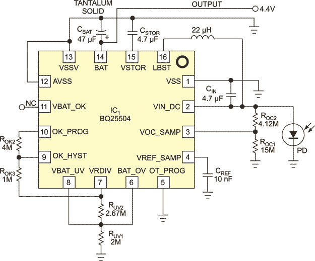
| Figure 1. | By exploiting the inherent weights of VBAT_UV and VBAT_OV inputs as 2/3:1, you can save at least two precision resistors in many applications. (IC1 is shown from the bottom view since, if breadboarding, the package style requires connections from the bottom.) |
The circuit in Figure 1 differs from those shown in the bq25504 data sheet in that it exploits a feature of the bq25504: The reference voltage at VBAT_OV (overvoltage) is internally multiplied by a factor of 3/2, as compared with the reference voltage at VBAT_UV (undervoltage). If limiting the battery voltage within an interval of VBAT_UV and (3/2)×VBAT_UV suits your application, you can connect the VBAT_UV and VBAT_OV inputs as shown in the figure and use a single resistor divider network for both, instead of two separate divider networks.
Thus, not only do you save two resistors, but you also can lower the value of the sum of resistances as RUV1+RUV2=4.67M without sacrificing the overall power efficiency of the circuit. As a by-product, you get a higher insensitivity to EMI at the VBAT_UV and VBAT_OV inputs.
The bq25504 has an ability to draw the maximum possible power from an input source. A photovoltaic cell, due to its nonlinear nature, outputs maximum power at about 80% of its open-circuit voltage. Resistors ROC1 and ROC2 determine this operating point of the solar cell, PD. This novel IC even tracks the chosen source operation point slowly to get as much power as possible under varying input source capability.
Experiments were performed with a single solar cell of diameter D=7.5 cm positioned horizontally on a desk located 1 meter from a window. Although it was sunny outside, practically no direct sunlight passed through the window. Under these circumstances, the short-circuit current, ISH, of the solar cell was 16.27 mA. Note that the ISH of the same cell reaches a value of 300 mA when the plane of the cell is oriented perpendicularly to full-sun radiation. With no load on the converter, the output voltages VBAT and VSTOR varied from 4.396V to 4.404V. This ±0.1% variation can be attributed to the fact that the boost converter operates in discontinuous mode to compensate for self-discharge of the capacitors CBAT and CSTOR and then idles for a relatively long time. The solar-cell terminal voltage was 0.441V with the converter unloaded.
When a 10-kΩ load resistor was connected to the VBAT output, this “wavering”of VBAT and VSTOR disappeared, and both become a constant 4.4V. The dc component of VIN_DC dropped to 0.4073V. By increasingly shadowing the solar cell with a metallic plate and thus depleting the energy available, I was able to reach an operating point where the output voltage was still 4.4V, while the mean value of voltage at the photocell terminals had dropped to 0.336V. It can be assumed that at this point the converter had entered a continuous-operation mode. (Note that even though the bq25504 data sheet shows VSTOR as the loaded output, in this application VBAT is used as the output because even a low output voltage is often better than none under energy-deficient conditions.)