Application Note TB3103
October 2013
Mihnea Rosu-Hamzescu
This technical brief describes a synchronous buck power supply, based on the PIC16F753 using 100% analog control for output regulation. The implementation has the advantage of not using any processor power, leaving the core free for more complex firmware. Also, the analog loop has a much faster response time to load steps and input voltage changes, making it useful for many applications.
The peripherals needed for the application are:
- One Complementary Output Generator (CWG)
- One Comparator (COMP)
- One Operational Amplifier (OPA)
- One 9-bit Digital-to-Analog Converter (DAC)
- One Fixed Voltage Reference (FVR)
- One Slope Compensation Module (SC)
- One Capture/Compare/PWM Module (CCP)
The peripherals are internally connected through firmware, significantly reducing the number of external pins needed for the implementation.
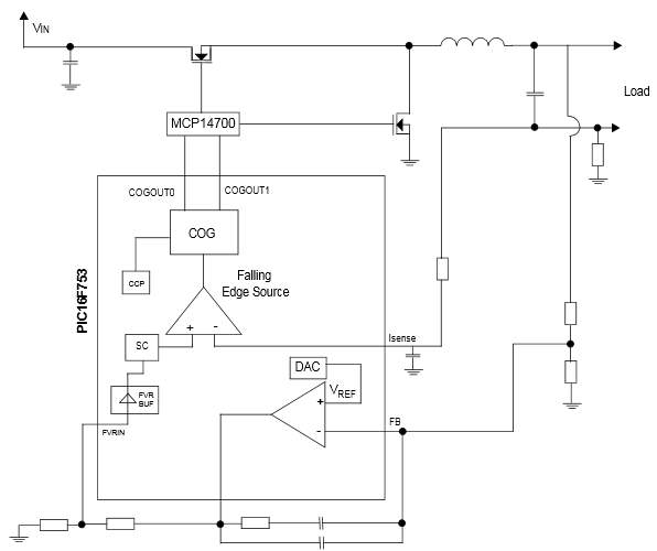
The output voltage is regulated using Peak Current mode control. The output voltage is compared to the reference voltage by the error amplifier (OPA) and the result is fed to the peak current comparator. The internal slope compensation module subtracts a software programmable ramp from the error amplifier output before the peak current comparator.
The CCP provides a fixed-frequency, fixed duty cycle control signal and the peak current comparator output is selected as a second (level-based) source for the COG falling edge.
![]() Download Application Note TB3103 (329 Kb)
Download Application Note TB3103 (329 Kb)

Figure illustrates the block diagram of the power supply
