R O Ocaya
EDN
When designing low-power USB circuits that require power-supply voltages other than 5 V, you must decide whether to use a separate battery or a physically small mains-based power source. The problem is particularly troublesome if the circuits to be powered require dual rails greater than 5 V, such as instrumentation amplifiers based on operational amplifiers, or must be run on portable computers, such as laptops.
The USB 2 standard specifies the power requirements of a connected device as either low power if it consumes at most 100 mA, or high power if it consumes up to 500 mA. The origin of the circuit described here is the design of a thermoluminescence (TL) instrument for which the microcontroller, the USB-interface controller, and 10 operational amplifiers are all powered from a standard USB port as a low-power device. The operation of the device requires high-efficiency performance with little noise pickup and keeping radio-frequency emission from the system as low as possible. The circuit was simulated before being built and verified and then used in the TL system. The design is attractive because its use of common components improves repeatability while keeping costs extremely low.
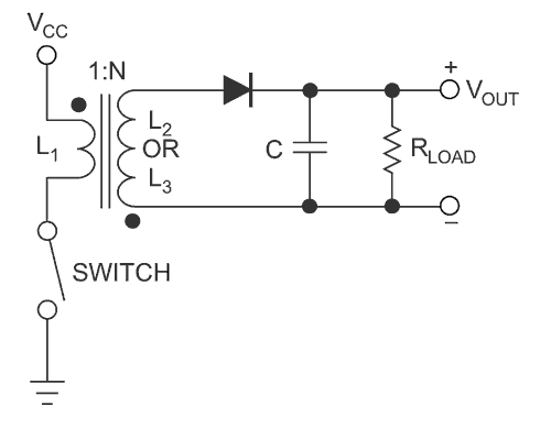
The operation is based on the flyback concept (Figure 1), where a small transformer is driven at 115 to 300 kHz generated by a pulse-width-modulated 555 astable circuit. The high frequency of operation allows the overall size of the circuit to be kept small while delivering relatively high power output with good regulation, and allows easier output filtering for low ripple.
In the actual circuit, you implement the switch using a MOSFET. In Figure 1, the diode is shown forward biased for positive VOUT. Reversing the diode direction and the polarity of one transformer winding gives a negative VOUT. The circuit operates in three distinct phases. In phase one, the switch is closed and energy is stored in a magnetic field due to current flowing in the transformer primary. The diode is reverse biased, and no current flows in the secondary.
 |
|
| Figure 1. | This basic flyback converter pumps magnetically stored charge into filter capacitor C when the switch opens. |
In phase two, the switch opens, the diode becomes forward biased, and the energy is transferred from the magnetic field into capacitor C. In phase three, with the energy dump completed, any residual charge stored on the switch drain-source capacitance is completely discharged. The cycle is then repeated.
To better explain the operation of the circuit, it is easier to presuppose that just prior to time t = 0, the filter capacitor is already charged to the nominal output voltage and that the current through the primary windings of the transformer is zero. At t = 0, the switch closes and a current starts to flow through the primary winding. This will induce a voltage across the secondary winding with a polarity as indicated. Since the diode is reverse biased, no secondary current can flow and the secondary winding is effectively open-circuit. The primary side of the transformer behaves like a simple inductor. As a result, the primary current increases linearly according to the following equation:
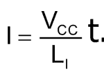
During the time the switch is closed, the voltage induced across the secondary windings is nVCC. The diode must therefore withstand a minimum reverse voltage of (nVCC + VOUT). At a given instant later, the switch is opened. In the practical circuit, this corresponds to the MOSFET’s being turned off. Suppose that the current in the primary winding at that instant is IPK. The magnetic energy stored in the inductor is then equal to

Due to the flux linkage between the primary winding and the secondary winding, with the primary circuit open, the inductor’s stored but collapsing magnetic field induces a voltage at the secondary side high enough (>VOUT) to forward bias the diode. The initial value of the current will be
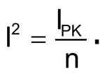
During the time that the diode is forward biased, the voltage across the secondary winding will equal (VOUT + 0.7). This can also be seen as a transformation of the primary-side voltage down to VOUT/n. The switch, therefore, has to withstand a voltage of effectively

when it is open. This last equation highlights the main advantage that the flyback converter has over the boost converter of comparable input and output voltages, namely the reduced voltage the switch must handle when it is opened. In effect, the voltage during the “off” phase is transformed down to a value determined by the transformer winding turns ratio. This allows a MOSFET with a much lower breakdown voltage to be used. Additionally, in the boost-converter topology, the diode must handle both the high “on” current and a high reverse voltage in the “off” phase. In the flyback converter, the diode at the secondary side has to withstand only a high voltage while the current is low (IPK/n). This permits the use of a diode with smaller capacitances that results in higher switching speed with the consequence of reduced energy losses and an increased efficiency.
Although it is beyond our current scope, you can calculate the output voltage by equating the amount of energy input in L1 to the energy transferred to the load, RLOAD. In steady state, the output is related to the duty cycle, D, of the switch and the frequency at which the switch is operated; that is, the open-circuit output voltage is given by

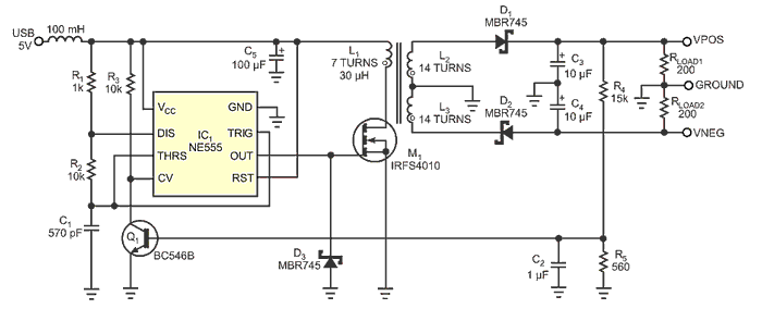
In the practical circuit of Figure 2, all of the elements of the basic flyback circuit of Figure 1 can be identified. However, there are a number of refinements that lead to better operation and stability. For example, two output diodes are configured so that dual-rail output is possible. Also, the positive rail feedback is sampled by the voltage divider comprising R4 and R5, with a level that is smoothed by capacitor C2. In normal 555 astable operation, the output waveform generation is possible since the timing capacitor (C1) charges from VCC through the sum of R1 and R2 and discharges through R2. With the resistor values used (that is, R2 >> R1), the duty cycle is close to 50%. The charging/discharging voltage levels are internally set to VCC/3 and 2VCC/3 (that is, 1.67 V and 3.33 V, respectively, if operated at 5 V). Without feedback, the values in Figure 2 give an open-loop output voltage of about 20 V.
 |
|
| Figure 2. | In this complete circuit, you can use many alternatives for M1, Q1, and the Schottky diodes. |
The feedback operates as follows: The transistor, Q1, does not conduct until the voltage at its base (VBE) is around 0.55 V. This enables the output voltage to be calculated from
As the output voltage continues to increase under the action of flyback, Q1 is driven even harder, causing its collector voltage to fall. Since the collector is connected to the control input of the 555 timer that is nominally the upper limit above (2VCC/3), this causes the capacitor to charge and discharge at the same rate but through a narrower voltage range. This has the effect of reducing both the “on” and “off” times of the output pulses that drive the MOSFET switch. The net variation in both the frequency and the duty cycle (D) causes VOUT to fall and eventually lower the feedback voltage, with the effect of reducing the “on” time of Q1.
One aspect of the circuit that needs careful setting up is the flyback transformer. Several home-made transformers were tried and worked reasonably well. The solution settled on was to reuse the core of an RFI suppression inductor commonly found at the mains input end of switched-mode power supplies in television sets. The windings of the transformer primary are multi-filar to reduce their series resistance. For example, using four strands of 0.3-mm insulated copper wire closely wound seven turns gave an inductance of 30 μH for the primary with a measured series resistance of 0.03 Ω. A lower coil resistance reduces joule heating in the inductor as it is switched, leading to higher efficiency. A suitable commercially available ferrite core and bobbin set is available from RS-Electronics (RS stock number 647-9446, manufactured by Epcos).
A further refinement is the use of high-current, high-speed, and low-forward-voltage Schottky diodes for D1 and D2. An additional diode is used in reverse bias at the gate of the MOSFET to reduce RFI. Including a 100-mH choke on the 5 V USB line also reduces switching noises further.
 |
|
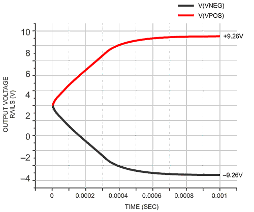
| Figure 3. | At turn-on, the output stabilizes within 0.8 msec, with two loads of 200 Ω each. |
For the purposes of our design, the USB port was modelled as a 5V source with a series resistance of 10 Ω for a worst-case current of 500 mA. A decoupling capacitor, C5, of 100 μF is used to prevent switching noises from being developed across the power rails. The measured output efficiency was around 72%, with a load of 50 Ω, with the output voltage dropping to ±7.6 V. The output has also been connected successfully to linear regulators such as the 78L05 for other voltages. A further design refinement is possible to make the output switchable under software control. We have not done it here, but some means of turning the 555 off or on using a separate active transistor would implement standby or active operation.
 |
|
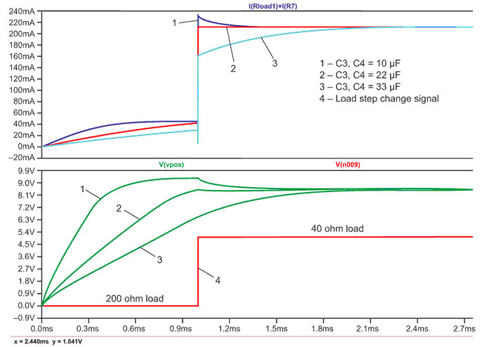
| Figure 4. | The circuit respond to a step load change 10 msec after turn-on. |
Figure 3 shows the turn-on transient response of the converter. Figure 4 shows that the circuit responds gracefully to a step load change 10 msec after turn-on.
