By Albert Wu, Linear Technology
EDN-Europe
In many electronic systems, it is necessary to provide a bipolar (positive and negative) voltage or current into a particular type of load. Loads that require bipolar voltages/currents include FPGA body biasing applications, thermoelectric coolers, DC motors, and many others.
There are many traditional methods to provide a bipolar voltage/current to a load. H-bridge designs are frequently used, but require that neither of the load’s terminals is tied directly to ground. Each of the load’s two terminals has to swing between the positive supply rail and ground and usually an inductor is placed in series with the load to filter out this chopped waveform. This lack of a direct ground connection to the load can complicate the mechanical and electrical design of the overall system. The H-bridge method also requires four switching elements and a more complex control scheme. There are loads that have a negative terminal that cannot be biased high relative to ground, such as an FPGA back-biasing application.
Another traditional method is to build two power rails, a positive one and a negative one. Various circuits are used to “swap” in the positive or negative rail with regulation to achieve bipolar voltage operation that can go below ground. This results in a very complex system, generally with poor efficiency, and a non-linear response at the point at which the output voltage crosses the ground potential.
A new DC/DC switching architecture is described here that has the ability to generate true four-quadrant operation, meaning the output voltage can be positive or negative and the current flow can be in either direction as well. Additionally, this new architecture can generate an output voltage that transitions from one polarity to another, through the ground potential, smoothly and without any non-linearity from mode transitions.
Four-quadrant DC/DC converter
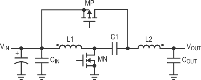
Figure 1 shows the basic connections and elements of the four-quadrant converter. NFET, MN and PFET, MP are operated out of phase from one another and at a constant switching frequency. Current mode control is used (not shown) to modulate the duty cycle of MN as needed.
 |
|
| Figure 1. | Four-quadrant DC/DC converter topology |
If we assume fixed frequency operation, the duty cycle for the ON time of MN can be calculated as
![]()
From this equation, it is clear that with a positive VIN voltage, the output voltage VOUT can be positive (up to VIN) or negative (limited only by practical DC considerations) and can go to 0 V as well. In fact, there is nothing special about the 0 V output level since the DC of the converter is 50% at that operating point.
The output of this converter can sink or source current regardless of the polarity of the output voltage, making this a true four-quadrant operating topology. The maximum drain to source voltage stress on MN and MP are both 2VIN – VOUT. For example, if VIN is +12 V and VOUT is –12 V, then the BVDSS ratings for both FETs must be greater then 36 V.
Four-quadrant topology device
The recently released controller from Linear Technology, the LT8710, can be used in the four-quadrant topology. Figure 2 shows a complete and fully tested circuit configured in this topology. The input voltage range for this circuit is typically 12 V, but allows a range from 11 V to 13 V. The output can be adjusted from +5 V to -5 V with an output current capability of ±3 A. An analogue control signal, VCNTL, is used to adjust the output voltage. The LT8710 is an 80 V capable controller so it can be used to build many other versions of the four-quadrant converter with higher or lower voltage and current capabilities.
 |
|
| Figure 2. | Four-quadrant converter using the LT8710. |
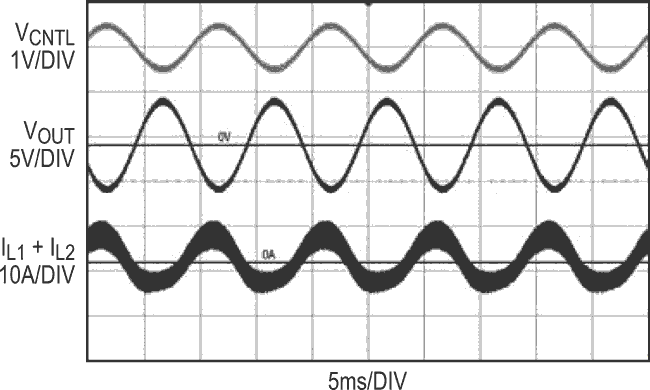
The four-quadrant operating capability of the converter is shown in Figure 3. Here, a sinusoidal control signal is used to generate a sinusoidal output voltage centred on 0 V. The inductor currents can go positive or negative; whatever is necessary to have the output voltage go to the commanded level. The operating waveforms show clean and smooth operation through the ground potential. The choice of using a sine wave control signal is arbitrary; a DC signal, square wave signal or any other type of signal could also be used.
 |
|
| Figure 3. | Sine-wave output voltage passes through 0 V. |
Applications
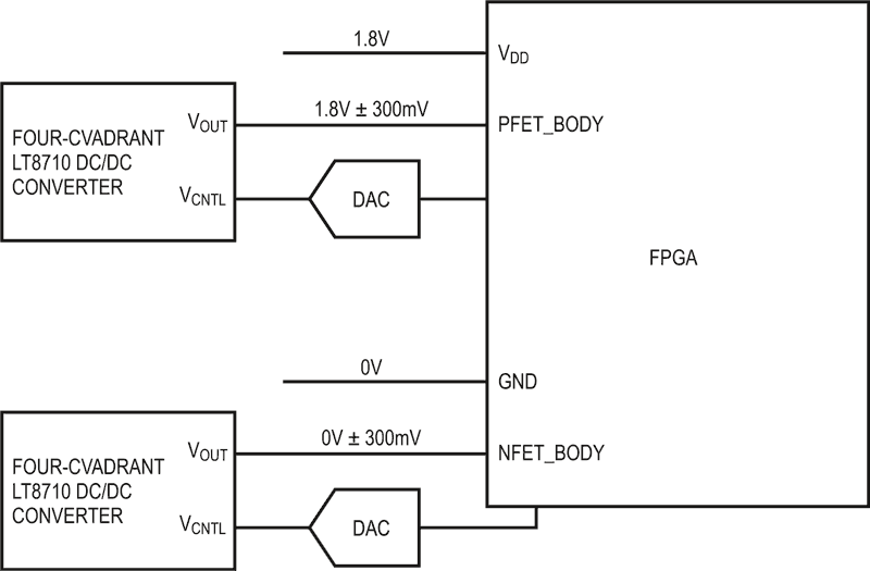
Many applications exist that can take advantage of this four-quadrant DC/DC converter. In high performance digital circuits, such as an FPGA, body back biasing can be used to significantly reduce static power dissipation while maintaining or improving dynamic performance. The voltage of the body of the PMOS and NMOS devices can be independently controlled in order to adjust the threshold (VT) of the devices. When the demands of the FPGA are low, the thresholds can be adjusted higher, significantly reducing leakage currents in the digital blocks. When demands are high, the thresholds can be decreased, increasing the speed and thus increasing the performance of the FPGA. Figure 4 shows a high level diagram of this application. Note that for the NMOS body bias, the voltages are typically 0 V ±300 mV and this is well suited to the four-quadrant topology.
 |
|
| Figure 4. | FPGA body bias application. |
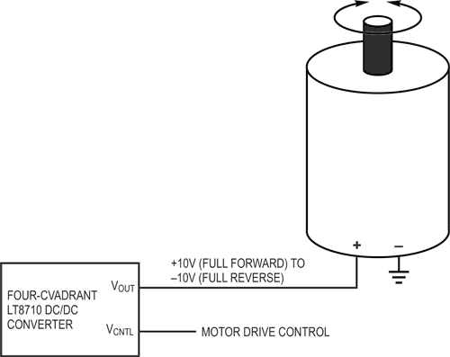
Another application that can benefit from the four-quadrant topology is DC motor drives. In many cases, DC motors need speed adjustment as well as reverse capability. The LT8710 used in the four-quadrant converter can do both. Figure 5 shows such an application. Note that the negative terminal of the DC motor can be simply tied to ground while the positive terminal can be adjusted between positive and negative 10 V. Similar to the DC motor drive application, the four-quadrant topology can also be used to drive thermoelectric coolers (TECs), audio speakers, and many other applications.
 |
|
| Figure 5. | DC motor drive with reversible drive direction. |
Conclusion
The LT8710 used in the four-quadrant DC/DC converter topology is a powerful circuit capable of producing positive and negative output voltages as well as positive and negative output currents. The inductor (L2 in Figure 2) in series with the output results in reduced output voltage ripple. Generating output voltages close to ground is also simplified since the duty cycle in this case is close to 50%. Many applications can benefit from this circuit, including but not limited to FPGA body biasing, DC motor drives, thermoelectric coolers, and audio drivers.
