Einar Abell
EDN
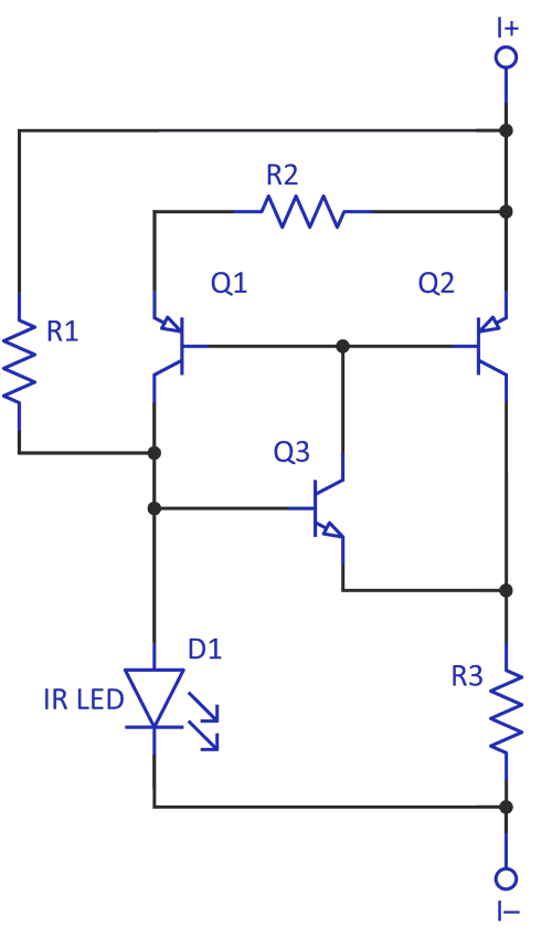
This Design Idea is a two-wire current regulator that strikes a good balance between performance and parts count. Employing three transistors, three resistors, and one LED, it achieves good regulation (better than 1% over most of the voltage range), lower operating voltage (1.2 V typical), and better tempco (0.07%/K) than other circuits of similar complexity.
It is designed to operate in a range of currents from tens of milliamperes to several amps. It does not use any hard to find parts; for example: an LM10 can be used to make an even higher performance circuit, but this IC is not multi-sourced and is likely to be discontinued.

An infrared LED is used as a ~1.05V reference, being driven by the bootstrapped current source of Q1. Q2 and Q3 form the main current regulator. R1 provides startup current, R2 sets the amount of reference current, and R3 sets the current through Q2, which controls 99% of the current through the regulator. At start up, all the current in R1 flows into the base of Q3, which in turn makes Q1 and Q2 conduct, providing more current to Q3. This continues until D1 begins to conduct and the current in R3 creates enough voltage to start turning Q3 off, creating negative feedback. Since Q3 regulates the current in Q2, it also regulates the current in Q1, which receives the same bias, but with the emitter resistor R2 scaling down the current. The current in Q1 and Q2 will now stabilize at a value set by R3, and to a lesser extent, R2.
Maintaining a constant current in Q1 requires that it be thermally coupled to Q2, since Q2 will dissipate most of the power in the circuit. The easiest way to do this is make Q1 the same transistor as Q2 and bolt both to opposite sides of a heat sink. Alternately, Q1 can be glued to Q2. For low current, a dual transistor is an option. A fourth option is to forgo thermal tracking, and achieve a measure of compensation by decreasing R1. Since the power dissipation in Q2 will be a function of the voltage, this will make the decrease in current in Q1 also a function of voltage, allowing compensation by R1. Unfortunately, all four methods will display a thermal transient with sudden power changes, the last method having the largest and longest.
The current in Q2 is set by the difference between D1's voltage and the VBE of Q3 (typically 0.3-0.4V) divided by R3:
![]()
The temperature coefficient of D1's forward voltage nearly matches that of Q3 (they differ by 0.25 mV/K), creating an overall tempco of approximately 0.07%/K for the regulator. Since R3 will typically be a few ohms or less, trimming the current is most easily achieved by trimming R2, which will change the current in D1, and consequently the voltage on R3.
R1 can be several megohms in most cases as the startup current is very small; when D1 is not conducting, the feedback is entirely positive. R2 is typically 200 to 300 ohms; the current in Q1 and D1 need only be a milliampere or so, even if the main pass current is a few amperes, as the gains of Q2 and Q3 multiply.
For the test circuit, current was down 5% at 1.2 V. This minimum voltage is set by VD1 and VSAT of Q1 and Q3. You should choose transistors with low saturation voltages (such as 2N3904 for Q3 and MJE210 for Q1 and Q2). This minimum voltage will change with temperature, decreasing at higher but increasing at lower temperatures. A PNP is used for the main pass transistor, but the circuit is easily converted to NPNs.
The regulator can be shut down by shorting D1; the current will drop to whatever flows through R1.
