Bench evaluation of transistors’ hFE may be needed during development of a system to ensure reliability of production systems. This circuit permits such testing using pulsed current and the biasing requirements set by transistor manufacturers.
The spread of hFE values in a batch of transistors may be wide enough to cause unreliable performance during mass production of a system. Consequently, bench evaluation of hFE may be required during the system’s development stage. Designers may have to screen samples over a spread of several years of date codes. Sometimes these measurements are made using pulsed collector current.
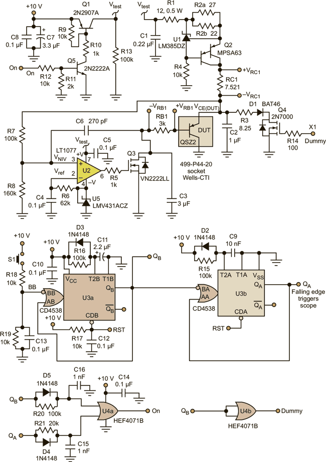
This idea describes how to make such measurements. For example, the QSZ2 transistor (2SB1695) specification states three biasing requirements on hFE: IC = 0.1 A, VCE = 2 V, and ∆tW = 1 ms. The circuit in Figure 1 meets these requirements for hFE measurement for a QSZ2 pnp transistor.
U1 and its associated components form a current regulator that sources 0.1 A to the succeeding stage. During the test period (∆tW in Figure 2), U2’s feedback mechanism trims the base resistance of the device under test (DUT) while maintaining its VCE at the required 2 V.
 |
|
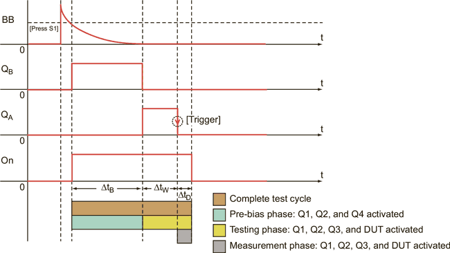
| Figure 2. | The actual test period is during the interval ∆tW, during which a 980-µs pulse is generated at QA. ∆tD (about 13 µs) ensures there is enough time to make the measurement. |
This is expressed in Equation 1, in which RDSQ3 is automatically tuned against IB(DUT) and, therefore, hFE and VBE(DUT) variations:
 |
(1) |
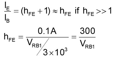
Equation 2 then allows you to determine the value of the DUT’s hFE by monitoring VRB1:
 |
(2) |
Basically, resistor RB1’s value is set as large as possible to minimize the oscillation of IB(DUT) upon transition and to maximize the signal level to ease VRB1 monitoring. The hFE of a QSZ2 ranges from 270 to 680, so IB(DUT) falls between 147 µA and 370 µA.
Next, assume the worst-case VBE(DUT) variation of 0.5 V to 0.8 V. Then:
 |
(3) |
 |
(4) |
Choose RB1 so that it is slightly below RB(min).
The circuitry around U3 forms two cascading one shots that, when triggered by S1, generate a 220-ms pulse (∆tB ≈ R16×C11) at the QB output. This is followed by a 980-µs pulse, ∆tW (determined by R15 and C9), at QA. The first pulse pre-biases and stabilizes the current source while the second one provides the needed test pulse for the DUT.
During ∆tB, Q4 is activated to sink the 0.1-A of U1, and R3 is selected so the effective voltage drop across R3, D1, and Q4 (and thus VCE(DUT)) is slightly less than 2 V (about 1.7 V in this example). This forces U2’s output and the DUT to stay “low” and “off,” respectively.
At the end of ∆tB, ∆tW starts and Q4 is turned off, transferring the test current to the DUT. U2 then raises VCE(DUT) to 2 V and regulates it.
 |
|
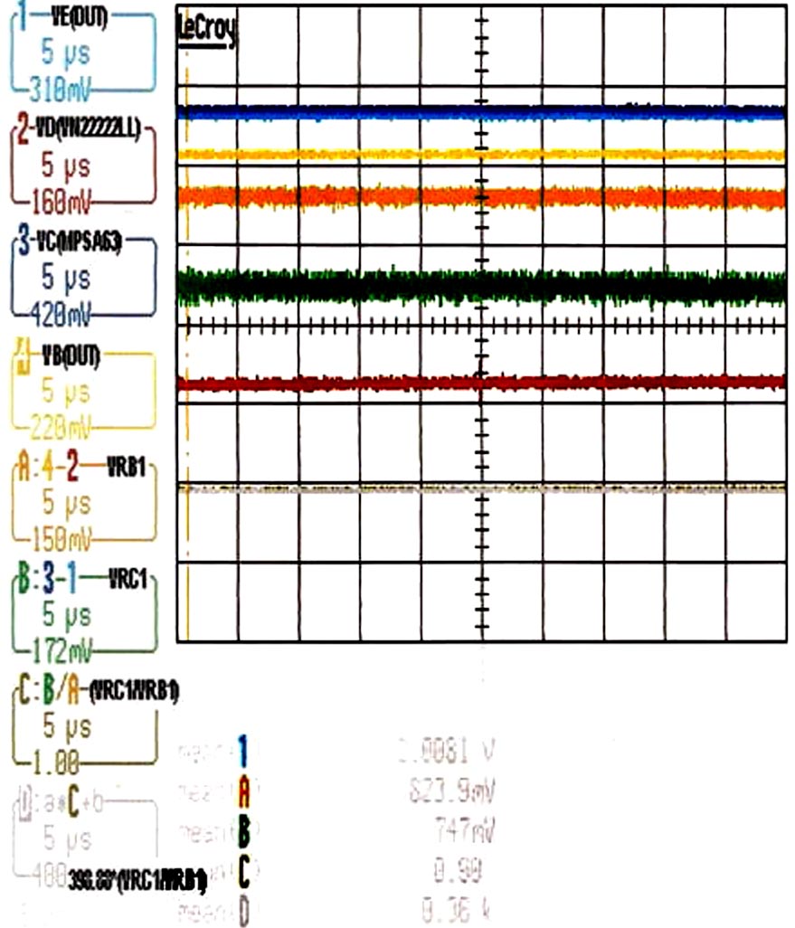
| Figure 3. | The falling edge of QA triggers an oscilloscope, which uses VRB1 (trace A) and VRC1 (trace B) to calculate hFE (trace D). |
The high-to-low transition at the QA output after ∆tW triggers the measuring device (in our example an oscilloscope). VRC1 and VRB1, which correspond to IC and IB of the DUT, are recorded upon QA’s trigger (Figure 3). R21 and C15 create ∆tD (about 13 µs), which ensures enough time to make the measurement before Q1 is gated “off.”

