When a MOSFET or IGBT gate-threshold voltage is higher than the available drive voltage, it's standard to use an op amp or other driver to bridge the difference. This circuit uses a basic optocoupler plus a few simple passive components to achieve the required results.
In some situations, it becomes necessary to drive a MOSFET (or IGBT) with a voltage that’s lower than its gate-threshold voltage (VTh). This is usually done with a driver or op amp to boost the signal to a level sufficient to drive the device. However, if the power-supply voltage powering the device is below or close to VTh, then even a rail-to-rail op amp will not be able to drive the MOSFET.
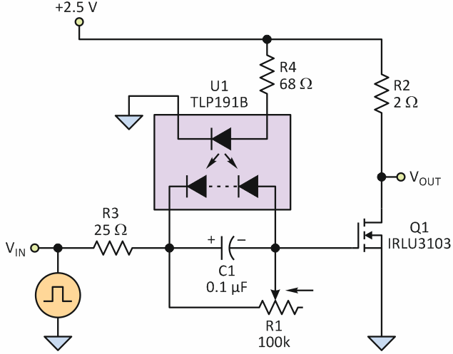
A simple technique can be used to drive a MOSFET with a signal that’s lower than VTh (Fig. 1).
 |
|
| Figure 1. | The optocoupler as a current source provides drive to a MOSFET gate with a voltage lower than the threshold voltage; R3 is the internal resistance of the test pulse generator. |
The isolated LED of optocoupler U1 is powered by the load supply (+2.5 V), and potentiometer R1 (100 kΩ) is connected at the output of the optocoupler. Since U1 is a photovoltaic coupler, it acts as a constant-current source up to a certain voltage, with the range determined by the device characteristics.
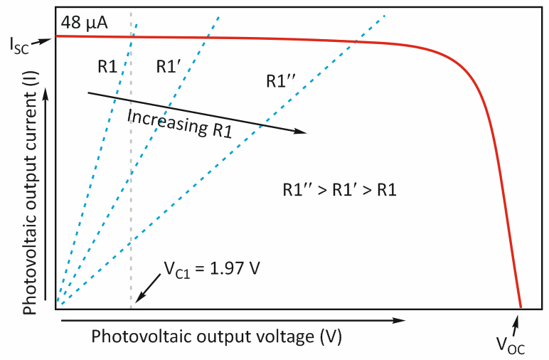
By changing the resistance of R1, it’s possible to bias MOSFET Q1 at various points to set different voltages at R1 (Fig. 2). With R4 set to 68 Ω, the LED forward current is set at approximately 16.5 mA, which provides short-circuit current ISC of the photovoltaic output of about 48 μA. Capacitor C1 ensures low signal-path impedance; its value should be much higher than the gate capacitance of MOSFET Q1. Here, we chose C1 = 0.1 μF, which is higher than the gate capacitance of the MOSFET being used.
 |
|
| Figure 2. | The output characteristic of the photovoltaic coupler shows that by adjusting the value of R1, the bias-point of the MOSFET can also be adjusted. |
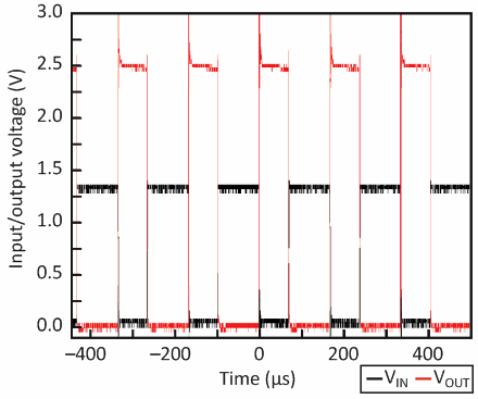
A resistive load, R2 (2 Ω), is used to test the circuit. R1 is adjusted to set the voltage close to the threshold voltage of Q1, which is measured as approximately 1.9 V. With the TPL191B, the maximum obtainable output voltage is about 7 V (VOC is approximately 8 V), which is above the threshold VTh of most devices. A signal generator is used to deliver pulses of amplitude about 1.2 V at the input (VIN); the signal generator has an internal resistance of 25 Ω (R3). Both input voltage (VIN) and output voltage (VOUT) are measured by an oscilloscope (Fig. 3).
 |
|
| Figure 3. | The relationship between input voltage and output voltage also shows slight on/off time delays, largely due to the internal resistance of the pulse generator used for test stimulus. |
The total input voltage to switch the MOSFET to the “on” state is 1.2 V + 1.9 V = 3.1 V, which is higher than the supply voltage (2.5 V). The small delay in off and on times (tOFF and tON) is primarily due to the pulse generator’s resistance (R3). A little overshoot occurs in the output voltage during switch-off, due to the load inductance. The 2-Ω load isn’t purely resistive, because it has a little inductance, too. It’s possible to use a smaller input signal (VIN) to switch a MOSFET, depending on the drain current and transconductance of the selected MOSFET.
This circuit works from dc to high frequencies, as set by the MOSFET. To see the effect with other MOSFETs, use LTSpice or any other simulation tool with a constant-current source in place of the photovoltaic coupler. In this case, use a current source of 48 μA.
References
