Guy Hoover, Linear Technology
Design Note 1034
Introduction
The high speed op amps required to buffer a modern 16 /18-bit analog-to-digital converter (ADC) typically dissipate as much power as the ADC itself, often with a maximum offset spec of about 1 mV, well beyond that of the ADC. If multiple multichannel ADCs are required, the power dissipation can quickly rise to unacceptable levels.
The simple buffer presented here is capable of driving the LTC®2372-18 8-channel ADC and achieving near data sheet SNR, THD and offset performance with very low power dissipation if the input signals involved are in the range of DC to 1 kHz.
Circuit Description
The LTC2372-18 is a low noise, 500 ksps, 8-channel 18 bit successive approximation register (SAR) ADC. Operating from a single 5 V supply, the LTC2372 18 achieves –110 dB THD (typical), 100 dB (fully differential)/95 dB (pseudo-differential) SNR (typical) with an offset of ±11 LSB (maximum) while dissipating only 27 mW (typical).
The LT6016 is a dual rail-to-rail input op amp with input offset voltage less than 50 μV (maximum) that draws only 315 μA per amplifier (typical). It is also available as a single and a quad (LT6015/LT6017).
 |
|
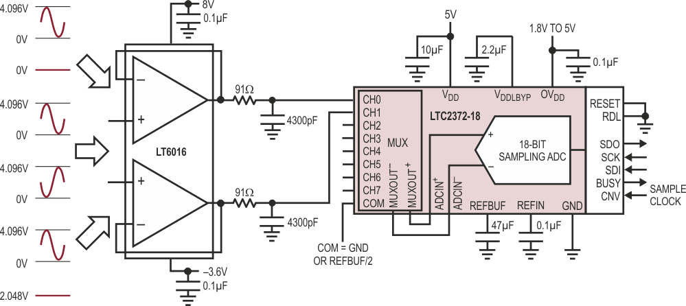
| Figure 1. | LT6016 Buffer Driving the LTC2372-18 8-Channel SAR ADC. |
The circuit of Figure 1 shows the LT6016 op amp configured as a noninverting buffer driving the analog inputs of the LTC2372-18. Typical power dissipation of each op amp is only 3.7 mW. For all eight channels this is a power dissipation of only 30 mW, approximately the same power dissipation as the ADC. Running the LT6016 on a single 5.25 V supply and enabling the ADC’s digital gain compression mode reduces the total op amp power consumption by more than half, to 13 mW, at the expense of a slight decrease in the SNR.
The RC filter at the buffer output minimizes the noise contribution of the LT6016 and reduces the effect of the sampling transient caused by the MUX and the input sampling capacitor.
Circuit Performance
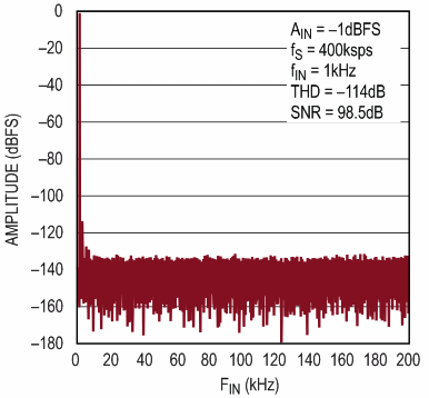
Figure 2 shows a 32768-point FFT of the LTC2372 18 driven fully differentially by the circuit of Figure 1. THD is –114 dB and SNR is 98.5 dBFS at 400 ksps, which compares well with the typical specs of the LTC2372-18.
 |
|
| Figure 2. | 32768-Point FFT for the Circuit of Figure 1. |
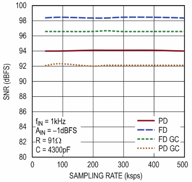
Figure 3 shows SNR vs sampling rate with digital gain compression off and on for both pseudo-differential and fully differential modes of the LTC2372-18. With digital gain compression off, the supply voltage for the LT6016 is +8 V/–3.6 V. With digital gain compression on, the LT6016 runs off a single 5 V supply. SNR stays fairly flat at 94 dBFS (pseudo-diff)/98.5 dBFS (fully diff) with digital gain compression off, and 92.1 dBFS (pseudo-diff)/96.6 dBFS (fully diff) with digital gain compression on, up to 500 ksps for all modes.
 |
|
| Figure 3. | SNR vs Sampling Rate for the Circuit of Figure 1 in Pseudo-Differential and Fully Differential Modes. |
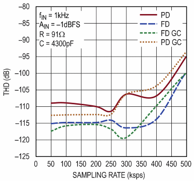
Figure 4 shows THD vs sampling rate with digital gain compression off and on for both pseudo-differential and fully differential modes of the LTC2372-18. Here THD starts to rise above –110 dB at 300 ksps for pseudo-differential mode and rises above –115 dB at 400 ksps for fully differential mode. Digital gain compression has only a minimal effect on the THD performance. In fully differential mode, THD is never worse than –100 dB up to the full 500 ksps sampling rate of the LTC2372-18.
 |
|
| Figure 4. | Pseudo-Differential, Fully Differential THD vs Sampling Rate for the Circuit of Figure 1 with and without Gain Compression. |
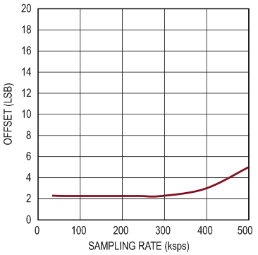
Figure 5 shows the combined offset error of the buffer and ADC vs sampling rate in pseudo-differential mode with digital gain compression off. Offset is initially less than 3 LSB and does not degrade until the sampling rate reaches 400 ksps.
 |
|
| Figure 5. | Offset Error vs Sampling Rate for the Circuit of Figure 1 in Pseudo-Differential Mode. |
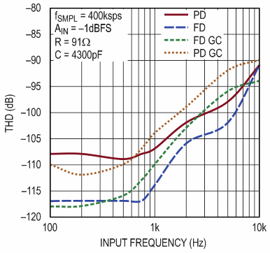
Figure 6 shows distortion vs input frequency for a 400 ksps sampling rate. Above 1 kHz, distortion rises for all modes.
 |
|
| Figure 6. | Distortion vs Input Frequency for the Circuit of Figure 1. |
Conclusion
A simple driver for the LTC2372-18 18-bit, 500 ksps, 8-channel SAR ADC – consisting of the LT6016 low power precision dual op amp configured as noninverting buffer is demonstrated. The driver dissipates only 3.7 mW per op amp (typical), and can be reduced to 1.6 mW by running off a single 5 V supply with the ADC in digital gain compression mode.
At sampling rates less than 300 ksps, SNR is measured at 94 dBFS (pseudo-diff)/98.5 dBFS (fully diff) with gain compression off and 92.1 dBFS (pseudo-diff)/96.6 dBFS (fully diff) with digital gain compression on; THD is measured at –110 dB (pseudo-diff)/–115 dB (fully diff) with digital gain compression off or on. Offset measures less than 3 LSB (pseudo-diff) with gain compression off. Above 300 ksps, performance gradually declines up to the full 500 ksps sampling rate of the LTC2372-18.
