Al Dutcher
EDN
This Design Idea provides a simple, inexpensive, portable circuit as an alternative to a microcontroller to provide a wide-range source of low-distortion sine waves for audio-circuit design and debugging. Although sine waves from DDS (direct digital synthesis) offer greater stability and fewer harmonics and other spurious-frequency components, this more "retro" approach lets designers use Linear Technology Corp's LTSpice freeware and hone their circuit-simulation skills. An oscillator comprises a frequency-determining network and a method of limiting oscillation amplitude to prevent circuit saturation, waveform clipping, and the generation of harmonics.
Many audio-oscillator designs use classic Wien-bridge bandpass-filter topology and include incandescent lamps, thermistors, or JFET circuits as amplitude-sensitive resistors to automatically vary feedback and limit amplitude.
However, amplitude-sensitive resistors introduce a small delay that can cause amplitude ringing while the oscillator stabilizes. In addition, the limiter's "soft" characteristics require frequency-determining components that track closely and maintain a level amplitude response over the oscillation range. Diode limiters present a softer characteristic than allowing an amplifier to go into "hard" limiting, and a diode limiter introduces no envelope delay. A Wien-bridge filter's frequency response rolls off relatively slowly and thus inadequately rejects clipping-induced harmonic frequencies. As a consequence, designers of most high-quality oscillators eschew the use of hard-clipping limiters.
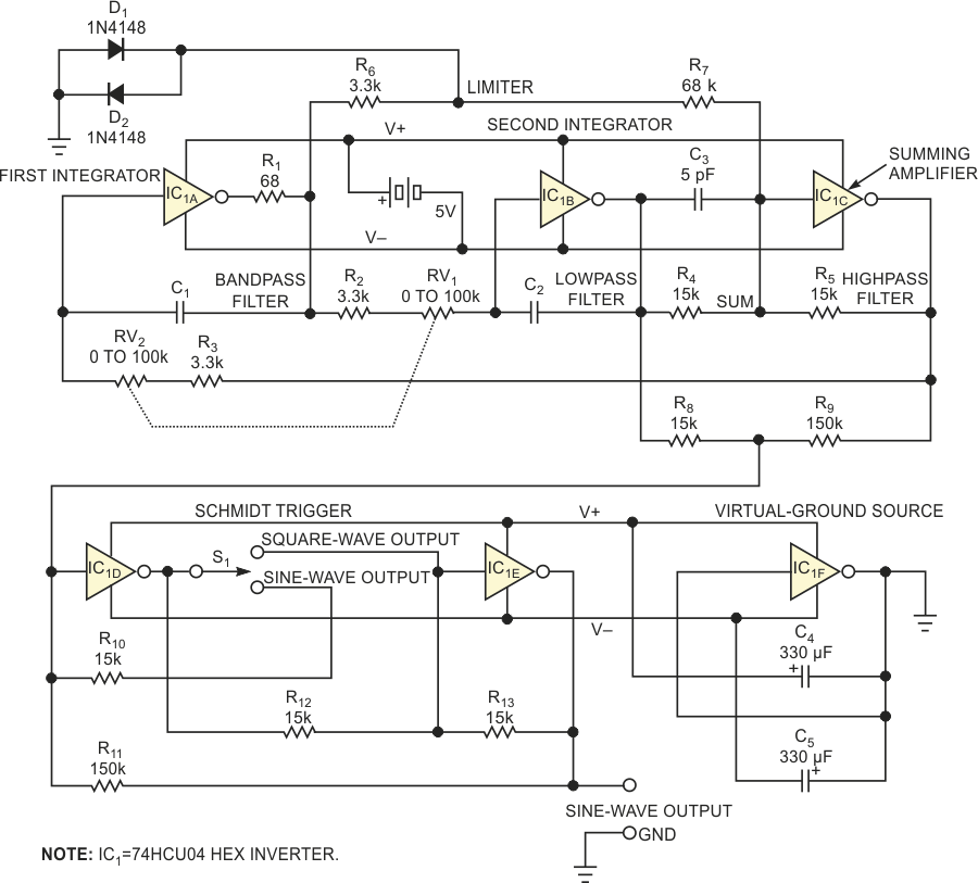
Figure 1 shows a sine-wave-oscillator design that makes unconventional use of a logic circuit. Based on state-variable topology that provides buffered highpass-, bandpass-, and lowpass-filtering nodes in one circuit, this oscillator relies on the peaking characteristics of an underdamped, two-pole lowpass filter that significantly boosts response at the fundamental frequency. In addition, the filter's lowpass node provides –12-dB-per-octave attenuation for harmonics. The state-variable loop comprises two integrators and a summing amplifier that provides 180° of phase shift. The two integrators each add almost –90° of additional phase shift, and the whole loop thus presents slightly less than 360 or 0° of phase shift and unity gain for oscillation.
 |
|
| Figure 1. | Build a sine-wave source around a single high-speed CMOS hex inverter and a handful of components. |
The loop's gain blocks comprise unbuffered 74HCU04 CMOS inverters that emphasize circuit simplicity, wide bandwidth, and self-referencing logic thresholds. Individual inverters each provide relatively low-voltage gains of approximately 15 per stage. Operating in Class A linear mode, the inverters produce no crossover distortion and thus produce harmonic amplitudes that decrease rapidly with harmonic order. In addition, a 74HCU04 package contains six inverters, making possible a one-device oscillator circuit.
To understand how the circuit operates, use the summing node at IC1C's input as a phase reference. Summing amplifier IC1C provides the first 180° of phase shift (inversion). Inverter/integrators IC1A and IC1B each present a quality factor, Q, equal to a gain of approximately 15, contributing a phase shift of –86° for a total of 180° – 86° = 94° each. The total phase margin for the three stages is 180° + 94° + 94° = 8°. The circuit's phase shift now amounts to 8° away from the "perfect" 0° phase required for oscillation. The total circuit Q of approximately 7.5 provides a boosted fundamental-frequency-filtering action of approximately 17 dB, but, at 8° phase shift, the circuit does not oscillate.
To obtain the exact 360° phase shift for oscillation, apply a small amount of signal from the filter's bandpass tap, which operates at a phase angle of 180° + 180° – 86° = –86°. Combine the circuit's Q of 7.5 and attenuate the bandpass intermediate output's signal at the bandpass filter by a factor of four, and the circuit oscillates with adequate gain and phase margins. Due to its symmetric internal configuration, a CMOS-inverter circuit attempts to maintain a logic threshold of one-half of its supply voltage. However, an N-channel MOS transistor conducts more than its P-channel counterpart, and the logic threshold shifts slightly toward the negative supply rail. Because an imbalance would lead to asymmetry if you use it as is for limiting the oscillation's amplitude, a pair of back-to-back 1N4148 diodes, D1 and D2, serves as a symmetrical limiter, preventing the gates from clipping the bandpass filter's output.
Soft clipping eases the filter's performance requirements by producing a third-harmonic level of –17 dB at the clipper's output. The filter's response peaks at 17 dB at the oscillation frequency, and the lowpass node provides 20 dB of third-harmonic attenuation for a theoretical third-harmonic total rejection of –54 dB. In practice, the CMOS devices' gain and threshold characteristics depart from ideal performance, and, as a result, the circuit produces sine waves that approach 1% distortion at the lowpass node, an acceptable level for the intended application. Replacing the CMOS inverters with operational amplifiers would further enhance performance.
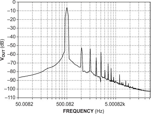
The filter's highpass node provides the first integrator's input signal, and the two cascaded integrators approach a 180° phase shift for all frequency components and also attenuate harmonic frequencies by a factor of 1/N2, where N represents the harmonic number. Subtracting some of the highpass signal, which contains harmonics produced by the diode limiter, from the lowpass signal further reduces the output's harmonic components. Resistors R8 and R9 form a 10-to-1 cancellation circuit that provides an additional 6-dB harmonic reduction for a 0.5% distortion figure at the signal output. Figure 2 shows harmonic levels for a 500-Hz fundamental output frequency.
 |
|
| Figure 2. | The oscillator’s output spectrum contains second- and third-harmonic levels of at least 250 dB below the fundamental. |
Oscillation occurs at unity gain at which the integrator's capacitive reactance equals the integrator's resistance, and at a frequency of 1/(2×π×R×C), where R = (RV1 + R2)=(RV2 + R3), and C = C1 = C2. For C = 10 nF and values of R of 8 to 80 kΩ, the circuit produces frequencies of 200 Hz to 2 kHz. You can use a 100-kΩ, dual-section ganged stereo-audio potentiometer as a frequency control. The control's ganged sections ensure that the integrators' resistance elements adequately track each other. To cover the audio spectrum of 2 Hz to 200 kHz, add a two-section band switch (not shown) to select pairs of capacitors with values of 1 µF, 100 nF, 10 nF, 1 nF, and 100 pF. You can use matched pairs of temperature-stable ceramic capacitors, but film-dielectric capacitors improve frequency stability. Compensation capacitor C3 improves output flatness at higher frequencies.
Over a typical frequency band, the output amplitude remains flat within 1 dB.
One of IC1's three remaining inverters, IC1F, serves as a virtual-ground generator by dividing the 5 V power supply, a floating four-cell stack of AA-sized nickel-cadmium or nickel-metal-hydride batteries. Current drain from the batteries averages 50 to 60 mA. Switch S1 connects the remaining inverters, IC1D and IC1E, to form a unity-gain buffer amplifier for sine-wave outputs or as a Schmidt trigger to produce a square-wave output. Resistor R11 sets the Schmidt trigger's hysteresis level. For ease of construction, use a perforated prototype board and the DIP version of the 74HCU04.
When you construct the circuit, note that the 74HCU04 can deliver appreciable gain at high frequencies, and excessively long leads can provoke parasitic oscillations that resistor R1 helps suppress by reducing gain at frequencies in the very-high-frequency range. If you reduce circuit values, this oscillator easily operates in the high-frequency range, and, although its stability doesn't approach that of an LC-based oscillator, the circuit offers easy adjustment over a wide frequency range.
