Jesus Rosales, Linear Technology
Design Note 545
Introduction
Industrial, telecom, medical and automotive applications use a wide variety of regulated voltages to operate effectively, including high voltage and negative rails. When the designer is faced with producing industrial power supplies, the job can be simplified by minimizing the parts count, as well as the number of required controller ICs. The LT8331 achieves both of these goals with an integrated 140 V, 500 mA switch, programmable frequency, ultra-quiescent current and light load Burst Mode® operation.
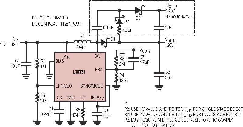
High voltage applications are easily accomplished using a simple boost converter, as shown in Figure 1. This application can output 120 V at 25 mA to 80 mA in a straight boost configuration or 240 V at 12 mA to 40 mA as a two stage boost by adding a few components, as shown inside the dotted line. The load can be taken entirely from VOUT2, or a combination of VOUT1 and VOUT2.
 |
|
| Figure 1. | 120 V or 240 V Output Boost Converter. |
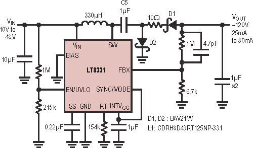
A high voltage negative output rail can easily be attained by configuring the converter as shown in Figure 2. This converter allows full switch voltage utilization to produce a negative output, by adding a capacitor and a diode. A coupling capacitor, C5, adds input to output disconnect during shutdown, similar to a CUK converter.
 |
|
| Figure 2. | –120 V Inverting Converter. |
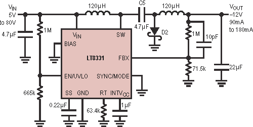
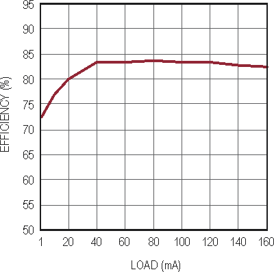
Figure 3 shows a CUK converter using the LT8331, and Figure 4 shows the efficiency curve for this inverter with a 12 V input. Efficiency for this converter peaks at 84%. Burst Mode operation kicks in when the load drops to about 40 mA, which allows the converter to maintain a respectable efficiency level of 73% even with a 1 mA load.
 |
|
| Figure 3. | –12 V Output CUK Converter. |
The LT8331 has very low quiescent current. It features an operation mode where the switching frequency is allowed to decrease progressively when a light load is detected. This mode enables the converter to maintain both high efficiency and low output ripple at light loads. The input current is just 29 μA when the output is unloaded and about 11 μA comes from the FBX resistor divider. If the converter is turned off by pulling the EN pin to ground, the input current drops to about 1 μA for a 5 V input, or 2 μA with a 12 V input. A good portion of the shutdown current is drawn by the EN/UVLO resistor divider.
 |
|
| Figure 4. | Efficiency Curve for Figure 3 (with a 12 V Input). |
The LT8331’s 4.5 V to 100 V input range and its 140 V rated switch make it an ideal candidate for SEPIC and CUK converters. Coupling capacitor, C5, breaks the input to output DC path, a desirable characteristic in applications where the output must be disconnected from the input. This has the added benefit of removing the current drawn by the FBX resistor divider. The switch voltage in these converters equals the sum of the input and output voltages.
Conclusion
The LT8331 simplifies the design of high output voltage and wide input voltage applications by reducing the number of external components. Its 140 V, 500 mA internal switch, 100 V input, programmable frequency, ultra-low quiescent current and light load Burst Mode operation make it ideal for a broad range of applications.
