J Jayapandian
EDN
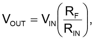
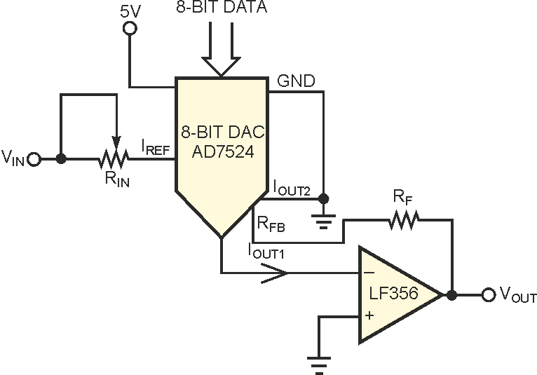
Numerous programmable-gain amplifiers are available, but a simple solution provides the option of using 256 gain steps with an 8-bit DAC and higher steps with higher bit DACs (Figure 1). According to the inverting-amplifier configuration of an op amp, the output voltage is

where RF is the feedback resistance, RIN is the input resistance, and VIN is the input voltage of the amplifier circuit. Generally, by changing the feedback resistance, you can get the desired gain.
 |
||
| Figure 1. | A DAC in series with an op amp attenuates the input signal to achieve the variable-gain factor. |
|
In this design, the 8-bit DAC in the input stage acts as a programmable attenuator for the input signal and permits a maximum full-scale IOUT1 of 1 mA. The value of IOUT1 is proportional to the input-voltage signal. The shunt feedback resistance, RF, converts IOUT1 to a voltage. Thus, the input signal, VIN, acts as a reference input to the DAC. Instead of increasing the value of the feedback resistor for higher gain, this circuit uses the DAC in series with the op amp to attenuate the input signal and achieve the desired variable-gain factor. You calculate the current output, IOUT1, from the DAC as follows, where D0 through D7 are the digital inputs to the DAC:

For example, if all of the bits are ones, the 8-bit digital image is FF, and the corresponding amplifier full-scale output is:

In an actual application, keep the value of RF fixed for the maximum gain. By varying the digital image pattern from 00 to FF, you can get the variable amplifier gain according to your requirements.
