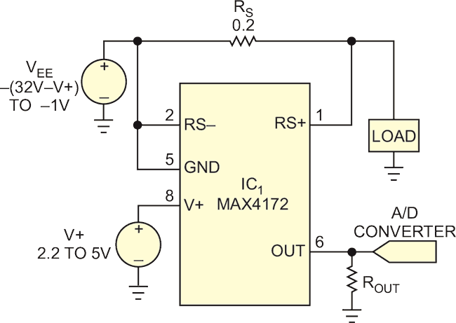
All dedicated current-sense amplifiers provide high-side sensing on a positive supply, but you can adapt such circuits for monitoring a negative supply (Figure 1). The positive-supply pin, V+, connects to the system's positive supply, and the ground pin, GND, connects to the negative supply, VEE. That arrangement monitors the negative supply and provides a positive output voltage for the external interface – typically, an A/D converter. The RS+ pin of the current-sense amplifier, IC1, connects to the load, and the RS– pin connects to the negative supply. IC1's current-source output drives a current that is proportional to load current flowing to ground, not to the GND pin. Output resistor ROUT converts the current to a voltage, which an optional ADC then digitizes.
 |
||
| Figure 1. | Connecting this positive-supply monitor allows it to monitor a negative current and generate a positive output voltage for the ADC. |
|
Saturation in the internal transistors, which occurs at approximately ((V+) – 1.2 V), limits the maximum output voltage. Thus, V+ must exceed the full-scale output by at least 1.2 V. If, for instance, the full-scale output is 1 V, then V+ ≥ 2.2 V. To meet the device's maximum and minimum operating voltages,
0 ≥ VEE ≥ – (32 – V+),
and
[(V+) – VEE)] ≥ 3 V.
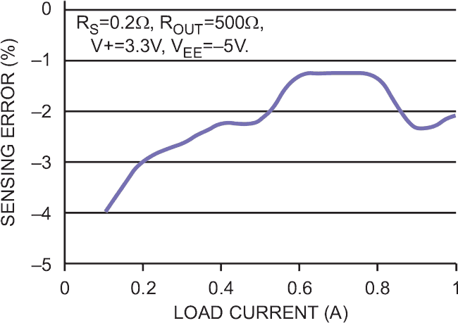
Figure 2 shows the variation of current measurement accuracy with load current.
 |
||
| Figure 2. | The current-sensing error of the circuit in Figure 1 varies with load current. |
|