Marty Merchant, Linear Technology
Design Note 470
Introduction
The LTCR3577/LTC3577-1 integrates a number of portable device power management functions into one IC, reducing complexity, cost and board area in handheld devices. The major functions include:
- Five voltage regulators to power memory, I/O, PLL, CODEC, DSP or a touch-screen controller
- A battery charger and PowerPath™ manager
- An LED driver for backlighting an LCD display, keypad and/or buttons
- Pushbutton control for debouncing the on/off button, supply sequencing and allowing end-users to force a hard reset when the microcontroller is not responding
By combining these functions, the LTC3577/LTC3577-1 does more than just reduce the number of required ICs; it solves the problems of functional interoperability – where otherwise separate features operate together for improved end-product performance. For instance, when the power input is from USB, the limited input current is logically distributed among the power supply outputs and the battery charger.
The LTC3577/LTC3577-1 offers other important features, including PowerPath control with instant-on operation, input overvoltage protection for devices that operate in harsh environments and adjustable slew rates on the switching supplies, making it possible to reduce EMI while optimizing efficiency. The LTC3577-1 features a 4.1 V battery float voltage for improved battery cycle life and additional high temperature safety margin, while the LTC3577 includes a standard 4.2 V battery float voltage for maximum battery run time.
Pushbutton Control
The built in pushbutton control circuitry of the LTC3577/ LTC3577-1 eliminates the need to debounce the pushbutton and includes power-up sequence functionality. A PB Status output indicates when the pushbutton is depressed, allowing the microprocessor to alter operation or begin the power-down sequence. Holding the pushbutton down for five seconds produces a hard reset. The hard reset shuts down the three bucks, the two LDOs and the LED driver, allowing the user to power down the device when the microprocessor is no longer responding.
Battery, USB, Wall and High Voltage Input Sources
The LTC3577/LTC3577-1 is designed to direct power from two power supply inputs and/or a Li-Ion/Polymer battery. The VBUS input has selectable input current limit control, designed to deliver 100 mA or 500 mA for USB applications, or 1 A for higher power applications. A high power voltage source such as a 5 V supply can be connected via an externally controlled FET. The voltage control (VC) pin can be used to regulate the output of a high voltage buck, such as the LT3480, LT3563 or LT3505 at a voltage slightly above the battery for optimal battery charger efficiency.
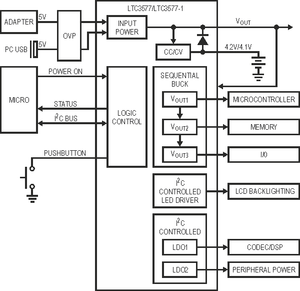
Figure 1 shows a system block diagram of the LTC3577/ LTC3577-1. An overvoltage protection circuit enables one or both of the input supplies to be protected against high voltage surges. The LTC3577/LTC3577-1 can provide power from a 4.2 V/4.1 V Li-Ion/Polymer battery when no other power is available or when the VBUS input current limit has been exceeded.
 |
||
| Figure 1. | Portable Device Power Distribution Block Diagram Featuring the LTC3577/LTC3577-1. | |
Battery Charger
The LTC3577/LTC3577-1 battery charger can provide a charge current up to 1.5 A via VBUS or wall adapter when available. The charger also has an automatic recharge and a trickle charge function. The battery charge/no-charge status, plus the NTC status can be read via the I2C bus. Since Li-Ion/Polymer batteries quickly lose capacity when both hot and fully charged, the LTC3577/LTC3577-1 reduces the battery voltage when the battery heats up, extending battery life and improving safety.
Three Bucks, Two LDOs and a Boost/LED Driver
The LTC3577/LTC3577-1 contains five resistor-adjustable step-down regulators: two bucks, which can provide up to 500 mA each, a third buck, which can provide up to 800 mA, and two LDO regulators, which provide up to 150 mA each and are enabled via the I2C interface. Individual LDO supply inputs allow the regulators to be connected to low voltage buck regulator outputs to improve efficiency. All regulators are capable of low-voltage operation, adjustable down to 0.8 V.
The three buck regulators are sequenced at power up (VOUT1, VOUT2 then VOUT3) via the pushbutton controller or via a static input pin. Each buck can be individually selected to run in Burst Mode operation to optimize efficiency or pulse-skipping mode for lower output ripple at light loads. A patented switching slew rate control feature, set via the I2C interface, allows the reduction of EMI noise in exchange for efficiency.
The LTC3577/LTC3577-1 LED boost driver can be used to drive up to 10 series white LEDs at up to 25 mA or be configured as a constant voltage boost converter. As a LED driver, the current is controlled by a 6-bit, 60 dB logarithmic DAC, which can be further reduced via internal PWM control. The LED current smoothly ramps up and down at one of four different rates. Overvoltage protection prevents the internal power transistor from damage if an open circuit fault occurs. Alternatively, the LED boost driver can be configured as a fixed voltage boost, providing up to 0.75 W at 36 V.
 |
||
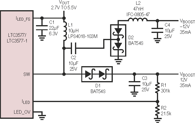
| Figure 2. | Dual Polarity Boost Converter. | |
Many circuits require a dual polarity voltage to bias op amps or other analog devices. A simple charge pump circuit, as shown in Figure 2, can be added to the boost converter switch node to provide a dual polarity supply. Two forward diodes are used to account for the two diode voltage drops in the inverting charge pump circuit and provide the best cross-regulation. For circuits where cross-regulation is not important, or with relatively light negative loads, using a single forward diode for the boost circuit provides the best efficiency.
Conclusion
The high level of integration of the LTC3577/LTC3577-1 reduces the number of components, required board real estate and overall cost; and greatly simplifies design by solving a number of complex power flow logic and control problems.
