The recent advent of Analog Devices ADCMP60x family of comparators has filled a gap between the less-than-1-µsec-response comparators consuming 100 to 200 mW and those exhibiting approximately 1-µsec response, requiring about one-thousandth that power. The ADCMP60x comparators exhibit a low value of the product of propagation-delay-by-supply-current drain; possess rail-to-rail input and output operation; and offer a variety of options for hysteresis, latch-mode operation, and shutdown mode. Some of them also have inherent level-translating capability. Moreover, the ratio of propagation delays for the positive and negative transitions at the output is close to the ideal value of 1 within 8 % tolerance for the ADCMP600, ADCMP601, ADCMP602, and ADCMP603 and with in a 6.7 % tolerance for the ADCMP608 and ADCMP609 members of the family.
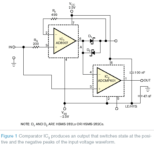
This ratio is important in applications in which both positive- and negative-output-level transitions are equally significant. Figure 1 shows one such circuit. Voltage-level transitions at the output of the detector indicate changing of the sign of the first derivative of the input signal; in other words, the circuit detects time positions of peaks and valleys in the input-voltage waveform. The detector circuit uses an ADCMP601 for IC2, and IC1 is an Analog Devices AD8007 current-feedback amplifier. IC1 connects as a voltage follower with an antiparallel combination of Schottky-barrier switching diodes, D1 and D2, between the output and the inverting input of the amplifier. Comparator IC2’s inputs connect to the source of the input voltage and to the output of the current-feedback amplifier. This configuration enhances the voltage difference of VIN–VA between inputs of the comparator. It performs this enhancement in a steplike manner at the instant, or region, at which the sign of slope of the input signal changes. This voltage difference is a measure of the double-forward voltage of diodes D1 and D2 at their forward current, which you derive from VIN/RF.

You use a current-feedback amplifier as IC1 because a dynamic current flows into its inverting input even when you connect it as a voltage follower. The values of the RS and RF resistors are those that Reference 2 recommends for a gain of 1. You needn’t worry about instability due to the presence of antiparallel diodes in the feedback path of the current-feedback amplifier. These diodes increase the value of feedback resistance to more than 499 Ω. Whenever the input voltage is only approximately 0V, the frequency-gain response of IC1 for an RF value greater than 499 Ω remains flat.

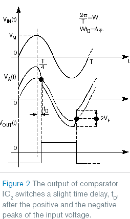
An analysis of the response of the voltage follower in Figure 1 to a harmonic input voltage uses ω/ωT and ω=2πf, where f is the input-voltage frequency and ωT is the radial transition frequency of the amplifier. At the radial-transition frequency, the ratio of ZM (the magnitude of the amplifier’s transimpedance) to RF drops to one. This simplification leads to an equation for the delay, tD, in
Figure 2:

where VF is the forward voltage of diode D1, Vm is the amplitude of input voltage, Rm0 is the dc transresistance of the current-feedback amplifier, and ΔΦ is the electrical-error angle in radians. The period of input harmonic voltage, T in Figure 2, represents 2π radians. The final error of the detector is ΔΦ, which decreases by a factor of  . This reduction occurs because the necessary operating overdrive over the midpoint of the steplike transition in the VA(t) voltage that the comparator requires is more than an order of magnitude less than the value of VF.
