Double-Anode MOSFET Thyristor
Michael Shustov, Andrey Shustov, Tomsk
A double-anode MOSFET thyristor circuit with UHS, high input impedance, and extremely low losses is proposed.
Thyristor (triac) load switches, by force of nonremovable specific design features, are characterized by a high cathode-anode drop on-state voltage and sluggish response. In this regard, a significant power is dissipated on such contact elements, sometimes resulting in overheating and failing the semiconductor device. At the same time, energy is wasted on useless heating a semiconductor device that leads to large-scale losses in the conditions of mass industrial and domestic application of thyristors and triacs.
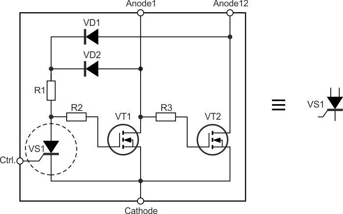
The double-anode MOSFET thyristor-controlled load switch (a double-anode MOSFET thyristor), depicted in Figure 1, has input characteristics of a high-speed thyristor, however, the losses on its open switching elements are almost twice as low as on traditional thyristors’. In addition, the switch proposed in contrast to thyristors, has two outputs, one is “on,” and the other is “off”. These outputs are switched according to switching thyristor.
 |
||
| Figure 1. | Internal pattern of double-anode MOSFET thyristor and its logic symbol. | |
The switch can be designed with an input low-current high-speed thyristor or its transistor analog with a high input impedance [1], the load of which is a high-ohm resistor. A serial strings of two high-current MOSFET transistor switches is connected to the thyristor anode.
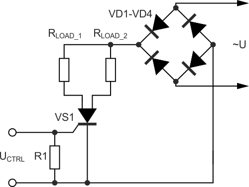
Figure 2 depicts a variant of a double-anode MOSFET thyristor practical use. When a rectangular control signal with a pulse-width modulation given to the switch input, a power rescheduling consumed in the thyristor MOSFET load circuits is possible without losses.
 |
||
| Figure 2. | Example of a double-anode MOSFET thyristor connection diagram in an AC circuit. |
|
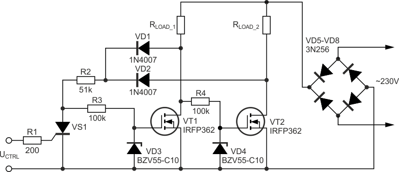
Figure 3 depicts a practical diagram of a load switch based on a double-anode MOSFET thyristor. Stabilitrons VD3 and VD4 are designed to protect the transistors’ control inputs from possible overstresses. The protective diodes in the source-drain circuit are built into the pattern of transistors IRFP362. N-channel MOSFET IRFP362 can operate up to a frequency of 1 MHz and are designed for a voltage of 400 V at a load current of up to 20 A; the source-drain resistance of an open transistor at a load current of 13 A is 0.25 Ohms.
 |
||
| Figure 3. | Practical diagram of a load switch with power rescheduling in a double-anode MOSFET thyristor load circuits. |
|
The upper frequency clipper of the switch supply voltage (1 kHz) is input thyristor VS1, as well as diodes VD1 and VD2. This frequency can be increased with higher-frequency thyristor VS1 or its transistor analog [1], as well as the choice of higher-frequency diodes VD1 and VD2 that is possible only at a rate effect.
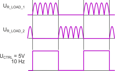
Diagrams of rectangular control signals with a voltage of 5V with the frequency of 10 Hz and the duty cycle of 50% and the corresponding output signals in the load circuits at the voltage of 230V, 50 Hz are depicted in Figure 4.
 |
||
| Figure 4. | Signal diagrams on control input and a double-anode MOSFET thyristor’s anodes |
|
When using a double-anode MOSFET thyristor in AC current with an adjustable power level in the circuit of one of its channels, unused in the case of classical thyristors “segments” of an AC current sine wave will not be wasted and can be applied in the circuit of its second load channel. In addition, the shape of the sinusoidal signal in the network will not be distorted by the uneven load on its “left” and “right” components.
The application of MOSFET as a part of the proposed variant of a double-anode thyristor provides its UHS, extremely low losses and high input impedance. That makes the double-anode MOSFET thyristor in its parameters closer to the perfect switching element.
