Martin Rowe
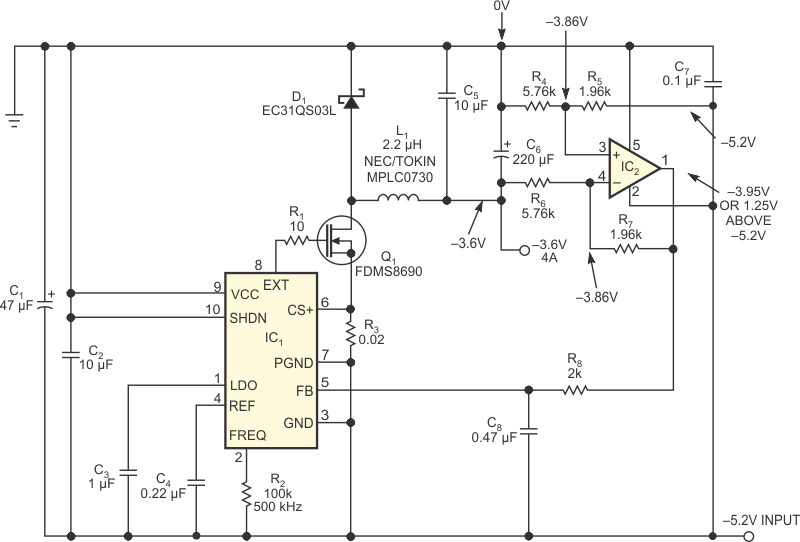
When converting a negative-output power supply to one with less-negative output, you must ensure that variations in input voltage don’t affect the output voltage. All such supplies include an internal reference voltage that enables output-voltage regulation. You usually refer this reference to the most negative rail, which is ground. Thus, the output voltage of such a converter depends on the accuracy of its negative input supply voltage. The circuit in Figure 1 lacks that limitation. Delivering output currents as high as 4 A with efficiencies better than 90%, it generates a negative output with the help of an op amp and a switch-mode boost converter. Closed-loop feedback regulates the output voltage with respect to ground, the most positive rail, which is also the node from which current is delivered to the load.
 |
||
| Figure 1. | A switch-mode converter generates a regulated negative supply voltage from a more-negative input voltage. |
|
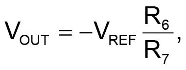
The circuit converts a –5.2 V supply voltage to –3.6 V. The boost converter, IC1 (MAX668), regulates its output voltage to maintain its feedback voltage at –3.95 V — 1.25 V above –5.2 V. Resistor R8 and capacitor C8 form a lowpass filter that stabilizes the voltage at FB. You must then select the R4/R6 and R5/R7 pairs to produce the desired output voltage. Making R4 and R5 equal and making R6 and R7 equal improves the common-mode performance. The ratio of R4 to R5 determines the voltage level at the positive input of op amp IC2 (MAX4322), whose closed-loop configuration ensures that the same voltage appears at its negative input. Knowing IC2’s output voltage, –3.95 V, and its negative input voltage lets you determine the output voltage using the values of R6 and R7:

where VREF is the 1.25 V nominal reference voltage of IC1, R4=R6, and R5=R7.
 |
||
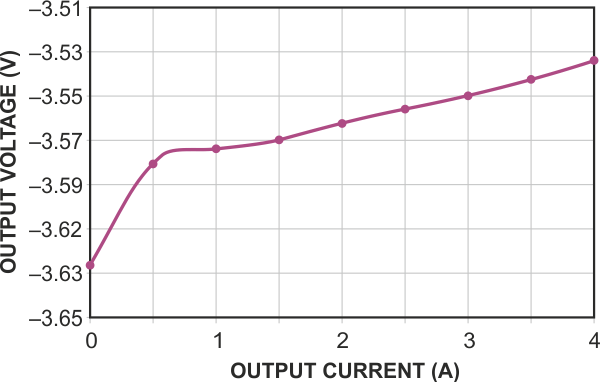
| Figure 2. | Output voltage for the circuit in Figure 1 varies with output current. |
|
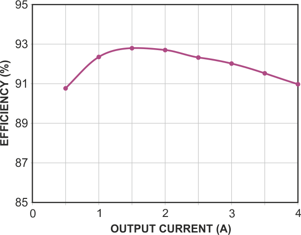
The component values in Figure 1 – for example, 1.96 kΩ for R5 and R7 and 5.76 kΩ for R4 and R6 – produce an output voltage of –3.76 V. Graphs of output voltage versus output current (Figure 2) and efficiency versus output current (Figure 3) illustrate this circuit’s performance.
 |
||
| Figure 3. | Conversion efficiency for the circuit in Figure 1 varies with output current. |
|
