Write Cycle
This is the simplest bus cycle. Target devices detect the start of the bus cycle by the FRAME# is asserted at the second clock. At a bus cycle is initiated, the bus comand and the address is taken in to each target device attached to the bus, and a terget device which detects the cycle is for oneself asserts DEVSEL# to answer to the bus cycle. In this case, because the target device answers by the one clock, it is high-speed decoding. When the device answers by second or third clock, it is midium or slow decoding.
After the terget device answered with DEVSEL#, the terget device confirms IRDY# is asserted (Write data is valid.), and takes data in the target device. At the same time, the target device knows that the transfer is the last cycle because of FRAME# is deasserted and IRDY# is asserted whitch means current data is last transfer.
When the last data is taken in, the terget device drives DEVSEL# and TRDY# to be deasserted, and DEVSEL# and TRDY# are released at the next clock, and the target device finishes the bus cycle.
.png)
Read Cycle
This is the simplest read cycle. As for the lead cycle, it needs one clock of buffer cycle because the agents who drive the AD bus is changed. Therefore, read cycle is compared in write cycle, and one clock much should be necessary.
Target devices detect the start of the bus cycle by the FRAME# is asserted at the second clock. At a bus cycle is initiated, the bus comand and the address is taken in to each target device attached to the bus, and a terget device which detects the cycle is for oneself asserts DEVSEL# to answer to the bus cycle. In this case, because the target device answers by the two clock, it is midium-speed decoding. It is necessary to put data on the bus at the 1 clock rest to change the agent for who not to do care and who takes a drive in the AD bus even if it answers by high-speed decoding.
After two clocks from start of the bus cycle, terget device puts read data on the AD bus, and assert TRDY#. At the next clock, terget device checks IRDY#. If the IRDY# is asserted (initiater can accept read data.), the data transfer is completed. And FRAME# is deasserted, it means current data is last transfer. Terget device detects it and terminates the bus transaction.
After last data is transferred, terget device drives DEVSEL# and TRDY# to deassert, and DEVSEL# and TRDY# are released at the next clock, and the bus transaction is terminated.
.png)
Write Cycle (Burst Transfer)
Burst transfer isn't distinguished from the single transfer. The terget device checks FRAME# at every data transfer. If the FRAME# keeps being asserted, terget device recoginizes next data to be transferred follows. The burst transfer is realized with this. The burst transfer is mainly applied to memory access, however, it can also be applied to I/O access.
PCI is designed to show performance most at burst transfer. It can be imagined easily from the address and data as well being multiplexed. At the burst transfer, terget address is only specified at start of data transfer is sufficient. PCI reduces the number of signal lines by this, and also reduces the stability of the operation and a cost.
.png)
Fast Back to Back Transaction
The method of first back to back transaction is defined to use a bus efficiently.
Usually, one clock of idol cycle exists between the bus cycles (transaction) at least. The idol cycle is a buffer time to prevent each output from colliding, however, it can be omitted when device switching is not occured between the bus cycles.
.png)
The Operation of the I/O Board : STATE
Because PCI is a complete synchronous bus, all operations are based on the system clock. The concept of state machine that a command from initiater is executed is necessary in a PCI board (target device) to be built. This I/O board realize the state machine with only one SPLD (GAL22V10). Next, let's make the value of state counter and the correspondence of the operation a figure, and explain.
.png)
STATE 4
Bus is in idol. The beginning of the new bus cycle is detected in this condition. It transits in STATE 2 or STATE 5 when an I/O cycle is initiated to this target device. It transits in STATE 0 when a bus cycle with no relations with this target device begins.
STATE 0
Bus is in non-idol. Any other transaction is executed. Wait until a bus becomes idol condition. It doesn't transit in the new cycle from this state.
STATE 2
An I/O write cycle to this device is being executed. This device asserts DEVSEL# and responds bus cycle. At the same time, terget device asserts TRDY# and shows that can accept data to be written. At this time, it latches data and transits to STATE 3 when IRDY# is being asserted (initiater can accept read data) and FRAME# is being deasserted (last data).
STATE 3
DEVSEL# and TRDY# is deasserted. Normaly, DEVSEL# and TRDY# are released at the next clock, and transits in the idol state (STATE 0). But, it transits directly in STATE 2 or STATE 5 without passing through the idol state when it faced this device under this state and I/O read/write command was issued again. (fast back to back transaction)
STATE 5
Start of read cycle. DEVSEL# and TRDY# is deasserted. Normaly, DEVSEL# and TRDY# are released at the next clock, and transits in the idol state (STATE 0). But, it transits directly in STATE 2 or STATE 5 without passing through the idol state when it faced this device under this state and I/O read/write command was issued again. (fast back to back transaction)
STATE 6
Read cycle is in progress. Terget device asserts DEVSEL# and respond to the read cycle. At the same time, output read data to the AD bus and assert TRDY#. At this time, it transits to STATE 7 when IRDY# is being asserted (initiater can accept read data) and FRAME# is being deasserted (last data).
STATE 7
Read cycle is finished. Terget device deasserts DEVSEL# and TRDY#. Then, release DEVSEL# and TRDY# at the next clock, and it transits to the idol state.
STATE 1
This state number is not defined. Even if it goes into this condition due to any error, it transits to STATE 0 at the next clock, and reverts to the normality loop.
The Design Rule Violation
Well, the circuit diagram is simplified in this experiment by partly omitting the function required as a PCI device. I explain about the omitted function, and the evil by that. It will specially never cause a trouble as an experiment made with a PC though they are the contents which faint when the designer of the normal PCI device sees it.
There is no configration register.
The existence of the device is recognized by a system by mounting configuration register. It realize to set up the function as a PCI device or to move terget address to avoid conflict.
The terget address is being decoded fixedly in this board without mounting configuration register. You must set up terget address so that the conflict of the resource may not occur because the existence of the device isn't recognized by a system. A PCI board with a DIP switch will be laughed :-)
There is no funftion of parity generation and check
A parity error surely occurs in read cycle because the check or drive parity signal aren't done. Any operation, such as NMI, occurs when parity error is detected when parity error respond bit of configuration register of Initiater (Host-PCI bridge) is set. But, it doesn't have an influence with the operation even if parity generator isn't mounted because that bit is usually 0 in the PC.
Upper 16 bits of address is not decoded
Only lower 16bit is being decoded by this board though 32bit full decoding is required with PCI with an I/O device as well. But, it is no problem because the access to the I/O space above 64K bytes doesn't occur in the PC.
Building the PCI Board
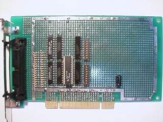
Circuit Diagram | PLD source fileThe proto-board for PCI is MCC-331(Sunhayato). It has a mount bracket, so that it is easy to use.
PLD should use the speed grade of 7ns or faster. Even 7ns doesn't satisfy specs with the specs of the bus timing. But, because to obtain the PLD faster than 5ns is difficult, it is used in consideration of the margin. (It will no problem.)
Any other parts except will not need to select manufacturer because they are the just ordinary. Inputs and outputs are 16bit for each because it lacked the mounting space of the connector this time though they were the places where 32bit wanted it respectively.


Circuit Diagram | PLD source file
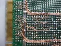
Because it is a digital circuit, I think that it never takes care of building. Because there is many wires, UEW is suitable for wiring. Don't use any other wire because it will become like a mountain. That you must be the most careful is not to mistake wiring. So it is easy to mistake because a terminal number is discontinuous at voltage key of the edge connector. I actually mistook some times, too. :-) Especially, a mistake of the power supply pins can destroy main board. Moreover, you should reinforce a power supply line fully because it operates at high speed of maximum 33MHz.
Test and Result
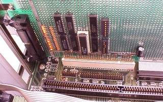
First, set the I/O address of this board with dip-switch. Because lower 2bit isn't being decoded, 4bytes that it continued is decided to be occupied. A bus will conflict when the I/O address duplicates with any other PCI devices at this time. It is needless to say that you must choose the I/O address which no one is using.
When for example F300h is set, this board responds to the access from F300h to F303h,

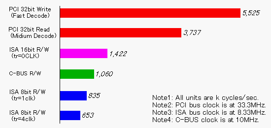
Well, let's go with the performance check if you can confirm that it operates completely. Performance test counts cycles per second that access terget device with I/O string operating instructions. The result is as follows:
Though it is natural, PCI showed an overwhelming speed in comparison with ISA. As for the write operation, 6clks/cycle, a read operation become 9clks/cycle's from the calculation of the number of clocks. But, because they are 3clks and 4clks respectively by the theory value, it will able to be said that a transfer rate doesn't rise that much, too. (Bus idol time is long.) Time loss in the HOST-PCI bridge thinks this a cause. However, PCI is designed so that the best performance may appear in the burst transfer. It is inevitable that performance is poor in the single transfer.
And, there is a difference in the speed which is near to the double in 16bit access and 8bit access in ISA bus. As for this, an I/O cycle is reduced when device responds as a 16 bit device in the ISA bus. It is good when even a 8bit device is made to operate -IOCS16 when it wants to increse a speed in ISA bus.
Notes
How was this report? PCI which it seemed to be complicated and which it didn't step into easily could be used with a means like an amateur, too. Though it seems generally to be complicated, you may have found that it operates based on the simple process surprisingly
