Batteries are the typical power sources for portable-system applications, and it is not unusual these days to find microcontroller-based portable systems. A variety of microcontrollers operates at low power-supply voltages, such as 1.8 V. Thus you can employ two AA or AAA cells to power the circuit. However, if the circuit requires higher voltage – for LED backlighting for an LCD, for example, which requires approximately 7.5 V dc – you must employ a suitable dc/dc converter to boost the power-supply voltage from, for example, 3 V to the required voltage. However, you can also employ a microcontroller to develop a suitable dc/dc-boost-voltage converter (Reference 1) with the help of a few additional discrete components.
 |
||
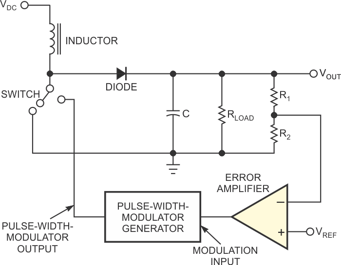
| Figure 1. | The output voltage in a boost switching regulator is more than the input voltage. The boost switching regulator operates in either CCM (continuous- conduction mode) or DCM (discontinuous-conduction mode) |
|
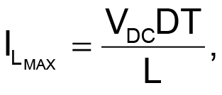
This Design Idea shows how to create not just one, but two dc/dc converters with just a tiny eight-pin microcontroller and a few discrete components. The design is scalable, and you can adapt it for a wide range of output-voltage requirements just by changing the control software for the microcontroller. You can even program the microcontroller to generate any required output-voltage start-up rate. Figure 1 shows the basic topology of a boost switching regulator. The output voltage in such a regulator is more than the input voltage. The boost switching regulator operates in either CCM (continuous-conduction mode) or DCM (discontinuous-conduction mode). It is easier to set up a circuit for DCM operation (Reference 2). The name comes from the fact that the inductor current falls to 0 A for some time during each PWM period in DCM; in CCM, the inductor current is never 0 A. The maximum current passes through the inductor at the end of high period of the PWM output (when the switch is on) and is:
 |
(1) |
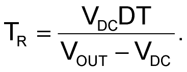
where VDC is the input voltage, D is the duty cycle, T is the total cycle time, and L is the inductance of the inductor. The current through the diode falls to zero in time TR.
 |
(2) |
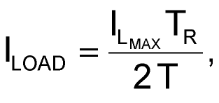
The load current is the average diode current,
 |
(3) |
from equation 1 and equation 2 and simplifies to:
 |
(4) |
The output voltage, VOUT, is:
 |
(5) |
The value of the output capacitor, which determines the ripple voltage, is:
 |
(6) |
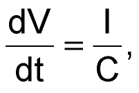
where dV/dt represents the drop in the output voltage during the period of the PWM signal, I is the load current, and C is the required output capacitor.
The total period of the PWM wave is T and is a system constant. D is the duty cycle of the PWM wave, and TR is the time during which the diode conducts. At the end of TR, the diode current falls to 0 A. The period of the wave is T > D×T + TR for DCM. The difference of the PWM period, T, and (D×T+TR) is the dead time.
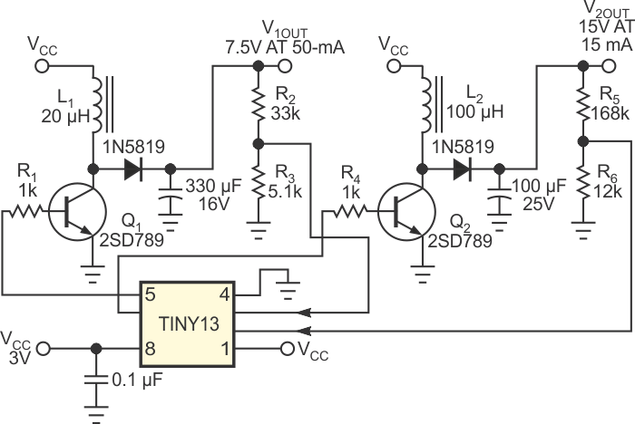
The switch that operates the inductor is usually a BJT (bipolar-junction transistor) or a MOSFET. A MOSFET is preferable because of its ability to handle large current, better efficiency, and higher switching speed. However, at low voltages, a suitable MOSFET with low enough gate-to-source threshold voltage is hard to find and can be expensive. So, this design uses a BJT (Figure 2).
 |
||
| Figure 2. | An Atmel ATtiny13 AVR microcontroller regulates two boost-dc/dc-converter outputs using its internal ADCs and PWMs. |
|
Microcontrollers offer PWM frequencies of 10 kHz to more than 200 kHz. A high PWM frequency is desirable because it leads to a lower inductor value, which translates to a small inductor. The ATtiny13 AVR microcontroller from Atmel has a “fast” PWM mode with a frequency of approximately 37.5 kHz and a resolution of 8 bits. A higher PWM resolution offers the ability to more closely track the desired output voltage. The maximum inductor current from Equation 1 is 0.81 A for a 20-µH inductor. The transistor that switches the inductor should have a maximum collector current greater than this value. A 2SD789 NPN transistor has a 1 A collector-current limit, so it is suitable for this dc/dc converter. The maximum load current achievable with these values, from Equation 4, is 54 mA and thus meets the requirement of maximum required load current for an output voltage of 7.5 V.
The ATtiny13 microcontroller boasts two high-speed PWM channels and four 10-bit ADC channels. Another PWM channel and an ADC channel create the second dc/dc converter for an output voltage of 15 V and a maximum load current of 15 mA. The inductor for this converter has a value of 100 µH. To calculate the output-capacitor value, use Equation 6. For a 5-mV ripple, the value of the capacitor for 7.5 V output voltage is 270 µF, because the output current is 50 mA and the PWM-time period is 27 µsec, so this circuit uses the nearest larger value of 330 µF. Similarly, for the 15 V output voltage, the required capacitor value is 81 µF, so the design uses a 100-µF capacitor.
The programs for the microcontroller are in C and use the open-source AVR GCC compiler. The AVR ATtiny13 microcontroller operates at an internal clock frequency of 9.6 MHz without an internal-clock-frequency divider, so the PWM frequency is 9.6 MHz/256 = 37.5 kHz. The internal reference voltage is 1.1 V. The main program alternately reads two channels of ADCs that monitor the output voltages in an interrupt subroutine. The main program executes an endless loop, monitoring the output voltage by reading the ADC values and adjusting the PWM values accordingly.
References
- “Boost converter,” Wikipedia.
- Pressman, Abraham I, Switching Power Supply Design, Second Edition, McGraw-Hill Professional, Nov 1, 1997, ISBN-10: 0070522367, ISBN-13: 978-0070522367.
- AVR GCC compiler