Many improvements to the follower circuit have been proposed over the years. The White cathode follower doubles the output current and makes the transfer function more linear. [1] Adding a common-base amplifying stage (current follower) significantly improved the White follower’s power-supply rejection ratio. [2]
Pioneer Electronic Corp. engineers took the next step by applying the White follower to a pair of followers connected in series. The premise of the Pioneer Super Linear Circuit (SLC) is that the nonlinear transfer function of the first transistor is canceled by the inverse nonlinearity of the second transistor in series. [3]
 |
||
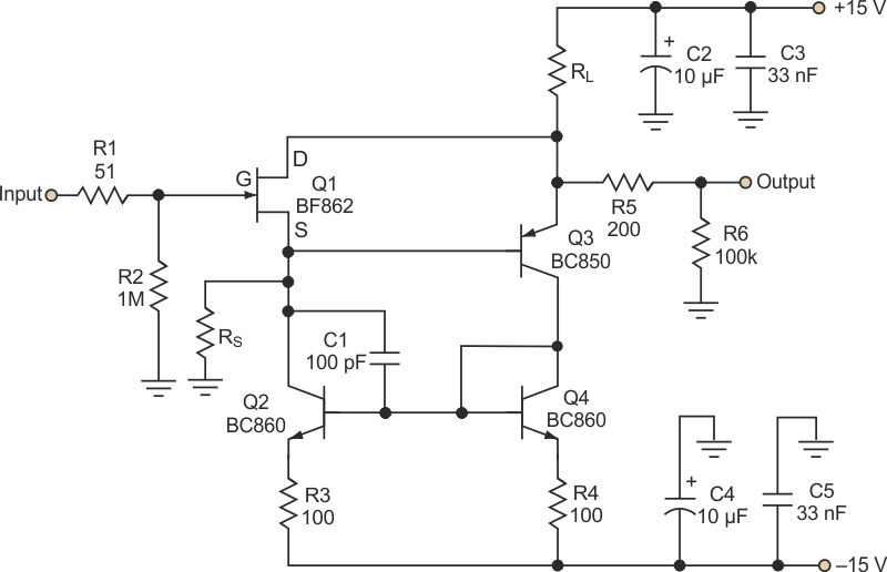
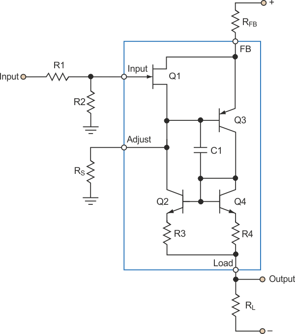
| Figure 1. | A JFET follower circuit with a current mirror made up of Q2 and Q4 provides distortion cancellation based on the value selected for RS. |
|
Figure 1 presents another improvement, a JFET follower with distortion compensation. Transistor Q1’s source voltage reproduces the input voltage and then drives Q3’s base. Both Q1 and Q3 supply current in the load, RL. Because of the current mirror (Q2-Q4), Q1’s source current is equal to Q3’s collector current. The sum of Q1’s source current and Q4’s collector current is:
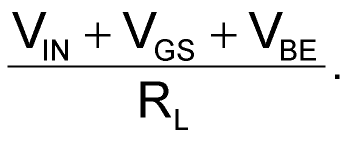
Because Q3 has a finite transconductance, its emitter current (or load current) will modulate its base-emitter voltage. The gate-source voltage of Q1 can be modulated in the same way by adding resistor RS to the SLC. At a certain value of RS, modulation in VBE will be cancelled by the same modulation in VGS. A similar distortion-cancellation mechanism occurs in a single-FET, common-source amplifying stage. [4]
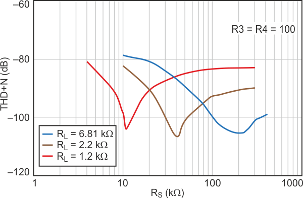
Figure 2 shows the measured total harmonic distortion plus noise (THD+N) for this circuit for three values of RL as RS is varied. The improvement is quite remarkable, with distortion for 1 V rms below 103 dB.
 |
||
| Figure 2. | For the three loads used in these measurements and at 1 V rms, THD+N is below 103 dB at the optimum RS. |
|
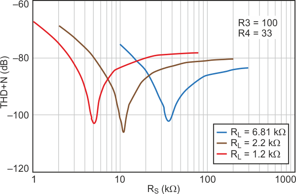
Another way to control the circuit’s balance condition is to change the current mirror’s transfer ratio. Figure 3 illustrates how the THD+N versus RS curves are shifted for a different ratio of R3/R4. In this case, Q1’s source current is a portion of Q3’s emitter current. This can be helpful when Q1’s quiescent current is determined by other design objectives – for example, noise performance.
 |
||
| Figure 3. | If the ratio of R3/R4 is changed, the required value of RS changes also. | |
Because of regenerative feedback, the capacitive load of Q3’s emitter will lead to high-frequency peaking inside the loop. So the load capacitance is isolated with R5, and some kind of frequency compensation (C1) might be needed. R6 = 100 kΩ represents the system input resistance.
 |
||
| Figure 4. | Because of the linear relationship of the output current and input signal created by the circuit, it can be rearranged in the form of an amplifier with a linear transfer function. |
|
The linear relationship between the voltage across RL and the input means there is a linear relationship between the output current and input signal. So, the circuit of Figure 1 can be rearranged in the form of amplifier with a linear transfer function (Fig. 4).
References
- White, E.L.C., “Thermionic Valve Amplifier Circuit Arrangements,” U.S. patent 2358428, Sept. 19, 1944.
- Taylor, P.L., “Audio Power Amplifier,” Wireless World, June 1973, p. 301.
- Ozawa, O., and Ishikawa, K., “Super Linear Circuit,” 60th AES Convention, May 1980, Preprint No. 1660, pp 1-38.
- Designing With Field-Effect Transistors, ed. by A.D. Evans, McGraw-Hill, New York, 1981, Ch. 3-11, “Distortion in FET Amplifiers.”
