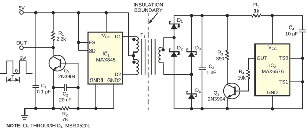
Temperature sensors must sometimes operate at locations whose return potentials differ considerably from that of the data-acquisition system's common – that is, equipotential – ground. In consequence, the temperature sensor's support circuitry must provide galvanic isolation between the sensor and its data-acquisition system. Also, the data-acquisition system seldom provides an isolated source of power for the sensor. The circuit in Figure 1 solves both problems by isolating the sensor's signal and power supply.
The complementary, fixed-frequency square-wave outputs of a power-transformer driver – IC1, a Maxim MAX845 – drive a Halo Electronics TGM-010P3 1-to-1-to-1 transformer with dual primary windings and a single untapped secondary winding. The secondary winding feeds a Graetz-bridge rectifier that generates approximately 4.5 V to power IC2, a Maxim MAX6576 sensor. Combining a temperature sensor, signal-processing electronics, and an easy-to-use digital-I/O interface in a low-cost package, the MAX6576 draws little current from a single supply source and maintains its specified accuracy over a 3 to 5 V supply-voltage range.
If you connect the sensor as Figure 1 shows, it operates as an absolute temperature-to-period converter and provides a nominal conversion constant of 10 µsec/K, which, at room temperature, yields a period of approximately 2.980 msec – a frequency of 335 Hz. You can adjust the conversion constant from 10 to 640 µsec/K. Note that longer conversion constants allow more signal-integration time to minimize noise effects. The sensor's symmetrical square-wave output drives NPN transistor Q2’s base through R4, a 10-kΩ resistor. A 390 Ω resistor, R3, serves as Q2’s collector load and connects to the same lines that deliver power to the temperature sensor. When Q2 conducts, it draws an asymmetrical power-supply current that exceeds the supply current during the sensor output's positive half-cycle.
 |
||
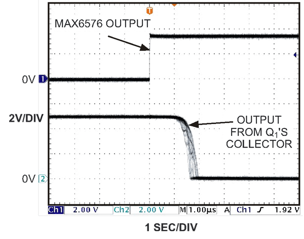
| Figure 2. | Measured from the positive-going edge of IC2’s output to the circuit’s output at Q1’s collector, the relative jitter averages less than 1 µsec. |
|
In IC1’s sensor output-to-ground return on the data-acquisition system's side, resistor R2 and capacitor C2 shunt Q1’s base-emitter junction. The values of R2 and C2 ensure that the sum of IC2’s current and transformer T1’s magnetizing current cannot drive Q1 into conduction. When Q2 conducts, it draws about 12 mA from the isolated 4.5 V power-supply line. Reflecting to the primary, Q2’s conduction current flows from the 5 V supply into IC1, out through its ground terminals, and partly through R2. The voltage drop across R2 exceeds Q1’s base-emitter voltage threshold and supplies sufficient base current to turn on Q1.
 |
||
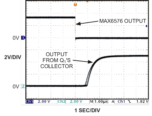
| Figure 3. | As in Figure 2, Q1’s average output jitter with respect to IC1’s negative-going output also averages less than 1 µsec. |
|
Thus, when Q2 conducts, so does Q1, which copies IC1’s isolated square-wave output to Q1’s collector circuit. As the waveforms of Figure 2 and Figure 3 show, Q1’s output rise and fall times, jitter, and propagation delay total about 2 µsec. The equivalent measurement error due to timing jitter amounts to less than 0.1 K at the fastest conversion constant of 10 µsec/K. Varying the circuit's supply voltage through a range of 4.5 to 5.5 V introduces an error of less than 0.1 K. The output at Q1’s collector can sink several milliamperes at a voltage excursion of 0 to 5 V.
This design can accommodate temperature-to-frequency converters and other types of temperature sensors.
