EDN
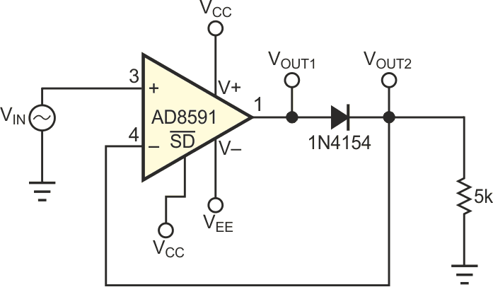
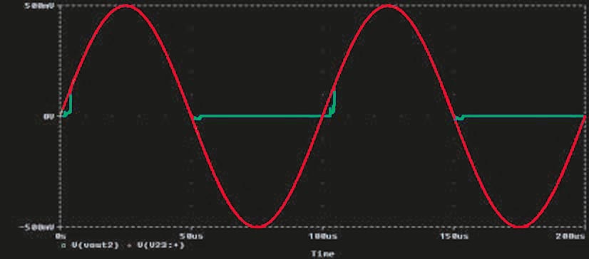
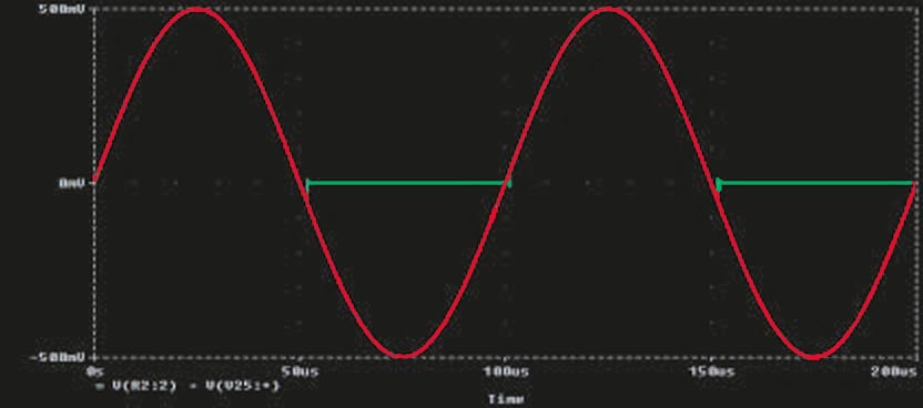
Rectifiers convert ac signals to dc. You can combine a diode and a load resistor to create a half-wave rectifier, provided that the amplitude of the ac source is much larger than the forward drop of the diode (typically 0.6 V). Unfortunately, you can't use this method to rectify signals that are smaller than a diode drop. For these applications, active rectifiers using amplifiers are available. The diode is inside the feedback loop of an amplifier (Figure 1). For VIN >0 V, the diode provides negative feedback, and the output, VOUT2, follows the input (VOUT2 = VIN). For VIN < 0 V, the diode does not conduct, the amplifier is in an open-loop configuration, and VOUT2 ~ 0 V. Figure 2 shows the response of the circuit in Figure 1. The output is shown in green; the input is shown in red.
 |
||
| Figure 1. | This circuit is a typical half-wave-rectifier configuration. | |
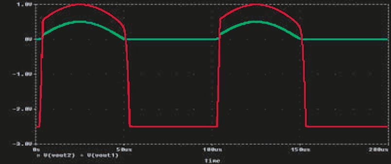
If VIN < 0 V, the amplifier behaves as a comparator. Its negative input is at a higher potential than its positive input, so its output, VOUT1, saturates to VEE. When the input again becomes positive, the amplifier has to recover from saturation and respond as quickly as its slew rate and saturation recovery time allow. This response takes some time, and the input may have changed by the time the amplifier is ready to respond to the positive input. The signals at VOUT1 (red) and VOUT2 (green) clarify this point (Figure 3). VOUT2 is the same waveform as in Figure 2. Note the change in scale factor. VOUT1 is a diode drop higher for positive inputs and saturates to VEE for negative inputs. The time delay in the response may result in a significant error in the output.
 |
||
| Figure 2. | These signals appear at the input (red) and the output (green) of the circuit in Figure 1. | |
 |
||
| Figure 3. | These signals are the waveforms at VOUT2 (green) and VOUT1 (red) in the circuit in Figure 1. | |
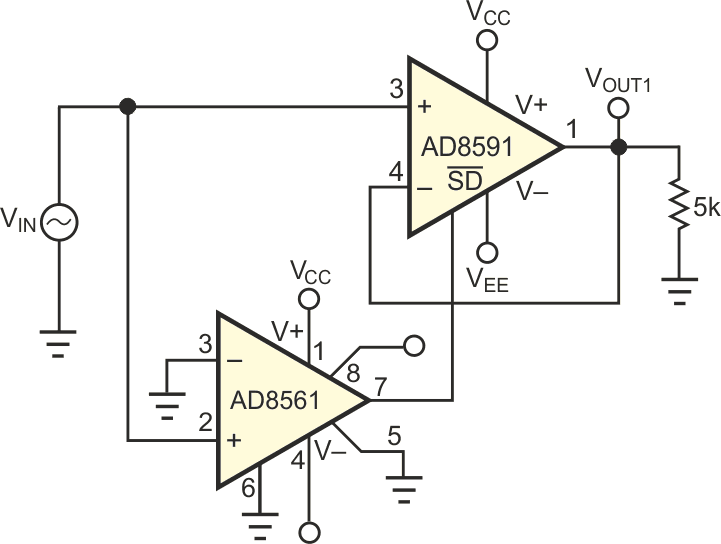
For example, an amplifier that has a slew rate of 2.5 V/µsec and saturates to –2.5 V takes at least 1 µsec to get ready to respond to positive inputs. During this time, the fast input has changed, so rectification starts at the wrong part of the input. One way to minimize this error is to use a high-slew-rate amplifier, but this solution comes at the expense of high power consumption. Another option is to use an inverting-amplifier configuration and two diodes, followed by a unity-gain inverting amplifier to obtain the noninverting rectification. This method appears in many textbooks. The circuit in Figure 4 represents a one-stage, noninverting rectifier that improves the accuracy of the rectification and reduces the power consumption. In this circuit, an AD8561 amplifier acts as a comparator. The AD8591 performs the rectification.
 |
||
| Figure 4. | This circuit greatly improves on the performance of the circuit in Figure 1. | |
When VIN > 0 V, the output of the AD8561 is high, and the AD8591 acts as a follower. When VIN < 0 V, the output of the AD8561 is low, and the AD8591 shuts down. This shutdown puts the output of the AD8591 into a high-impedance state, so it remains at approximately 0 V, rather than saturating to VEE as it did in the previous circuit. When VIN goes positive, the amplifier comes out of shutdown and again follows the input. This turn-on time (the time it takes to come out of shutdown) is much shorter than the saturation recovery time and slew-rate limiting that occurs in the previous circuit. Figure 5 shows the signals at the input (red) and output (green) of the improved rectifier circuit.
 |
||
| Figure 5. | These signals appear at the input (red) and output (green) of the circuit in Figure 4. | |