It seems deceptively simple to establish galvanic isolation with the help of optocouplers between circuits that operate at different ground potentials. Optocouplers draw power from the isolated circuit, and switching can be relatively slow and uncertain because of LED aging. Substitutes without optocouplers, such as the ADUM12xx from Analog Devices or ISO72x from Texas Instruments, are available. This Design Idea describes a method of improving the simple optocoupler.
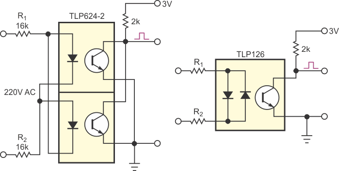
Figure 1 shows two popular designs of 0 V synchronization with ac. An attempt to reduce power draw from the isolated circuit by decreasing the optocoupler’s LED current with a corresponding increase of the optocoupler’s load resistor yields slower and more uncertain switching. To achieve faster and sharper switching, you would have to sacrifice power efficiency; however, the benefit of this sacrifice is limited because of the inverse relationship between power efficiency and the ac-voltage magnitude.
An optocoupler’s LED emits almost continuously during nearly all ac cycles exceeding the nominal, leading to low power efficiency and relatively fast aging of the optocoupler. One more drawback is excessively large and nearly uncontrollable zero-crossing error; the circuit’s sensitivity threshold depends on the parameters of the optocoupler. The designs in Figure 1 do not provide an ideal approach. With respect to efficiency, they can draw 5 to 100 mA, depending on the optocoupler’s current-transfer ratio and the ac amplitude.
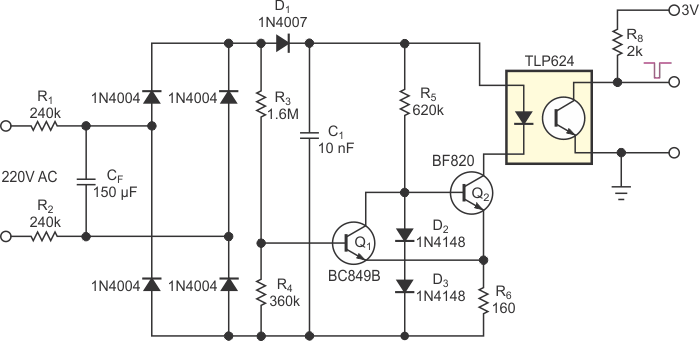
The design in Figure 2 overcomes the problems of excessive power consumption, uncertain switching, and LED aging. It lends itself well to wide-ac-range applications. Compared with the circuit in Figure 1, Figure 2’s LED emits only in close vicinity of the zero-crossing point and receives its power from the previously charged capacitor, so you can reduce the average current draw by a factor of 10 to 100. The design also provides faster, more deterministic, and sharper switching. What’s more, you can expect slower LED aging. Resistors R1 and R2 in Figure 1 dissipate no less than 1.5 W of power as waste heat, so changing them to 0.1 W devices allows placement of additional components on the same board area (Figure 2).
 |
|
| Figure 2. | This circuit overcomes problems of excessive power consumption, uncertain switching, and LED aging. |
The circuit’s main components comprise amplitude detector D1, capacitor C1, and Schmitt trigger Q1/Q2 to control a current through the optocoupler’s LED. D2 and D3 stabilize the base voltage of Q2 and, hence, its collector current, which activates the optocoupler. Capacitor C1 charges up through R1, R2, and D1.
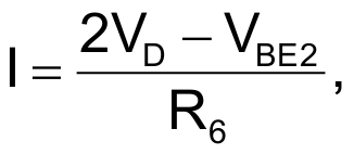
During nearly all of the ac-cycle time, except in the vicinity of the zero-crossing point, Q1 is on, and Q2 is off. Then, approaching the zero-crossing point, the state of Schmitt trigger Q1 and Q2 changes, and Q2 discharges capacitor C1 with the constant current, because the circuit comprising Q2, D2, D3, R5, and R6 stabilizes current as

where VD is the voltage drop on D2 or D3 and VBE2 is the base-emitter voltage of Q2.
 |
|
| Figure 3. | Another variant of this design shows how to manage without a requirement for minimal reverse current in D1. |
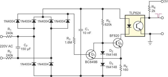
Some applications require none of the hysteresis that is inherent to a Schmitt trigger; Figure 3 shows such a design. It also shows how to manage without a requirement for minimal reverse current in D1. This circuit, however, better suits pure synchronization and not thyristor control. Because of the stability of LED current, these designs provide an expanded input-ac-voltage range, which may be useful for a multistandard ac-powered gadget; an opportunity to set the LED current without the risk of overloading the LED; and a reduced influence of the optocoupler’s instability. One more advantage of these designs is their inherently safer nature. In the case of a short circuit in their terminals, optocouplers deliver 10 to 100 times less current between the isolated and the nonisolated sides than the circuit in Figure 1. The optocoupler also offers advantages. Thanks to the low duty cycle, you can freely reduce the value of the optocoupler’s load resistor, R8, without sacrificing power efficiency. This reduction results in low zero-crossing error.
Materials on the topic
- Datasheet Toshiba TLP126
- Datasheet Toshiba TLP624
- Datasheet Nexperia BF820
- Datasheet Fairchild BC849

