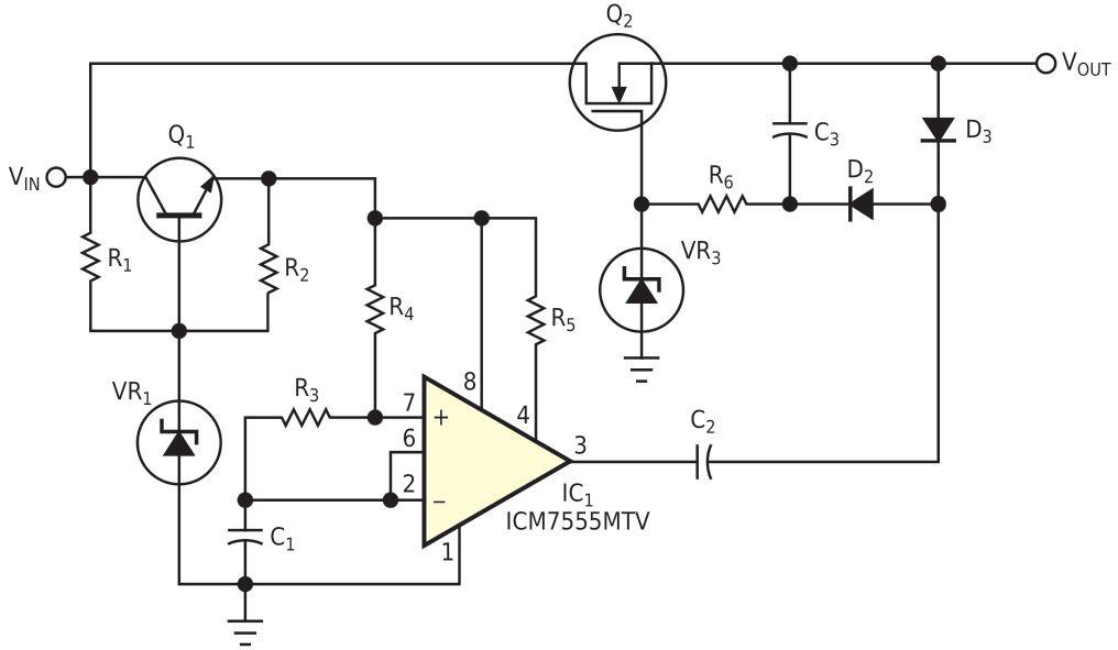
The circuit in Figure 1 is a quasi-linear regulator. It functions as a source follower for input voltages greater than a preset level, determined by VR3. For input voltages lower than the preset level, the pass element, Q2, operates as a saturated switch. The circuit comprises an oscillator, a charge pump, and a linear regulator. The linear regulator, consisting of Q1, R1, VR1, and R2, drives a charge pump comprising C2, D2, D3, and C3. The charge pump generates a voltage equal to the output of the linear regulator for input voltages greater than the breakdown voltage of VR1. For input voltages lower than VR1’s breakdown voltage, the output voltage is VOUT = VIN – IOUT×(RON of Q2). For input voltages that exceed VR3’s breakdown voltage by approximately 3 V, R6 and VR3 dissipate the energy the charge pump supplies. In this mode, the circuit functions as a source follower, and the output voltage is approximately 3 V lower than VR3’s breakdown voltage. The circuit dissipates minimal power. During transients, the load current determines the dissipation in Q2.
 |
|
| Figure 1. | This circuit clamps transient voltages and dissipates minimal power. |