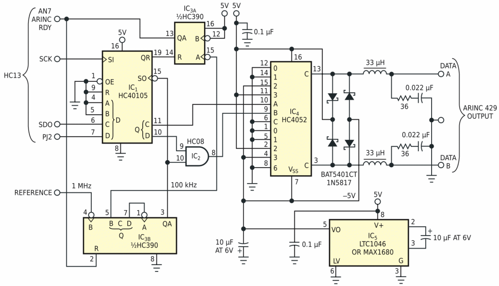
The ARINC (Aeronautical Radio Inc) 429 specification defines the air transport industry's hardware and protocol standards for the transfer of digital data between avionics systems. Circuitry that can implement elements of the 429 spec is often an essential part of control and sensor electronics intended for the aviation environment. ASIC chips for this purpose are commercially available, but they typically require nonstandard power supplies (for example, ±15 V) and wide parallel interfaces. Therefore, it's sometimes inconvenient to accommodate them in 5 V microcontroller-based designs. The circuit in Figure 1 serves the Tx (transmit/output) portion of the 429 spec. The design implements a high-speed ARINC-429-compliant transmit function using a single 5 V supply rail and 74HC series chips.
 |
|
| Figure 1. | This ARINC 429 transmitter operates from a single 5 V supply and meets all timing requirements of the 429 spec. |
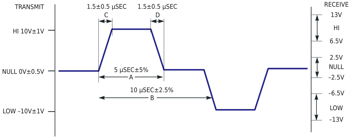
The physical transmission medium for the 429 standard is 78 Ω shielded, twisted-pair cable that uses a complementary, differential bipolar RZ (return-to-zero) waveform (Figure 2). The voltages are the net differentials that the biphase drive develops: For example, the differential is 10 V when you drive the Data A signal in Figure 1 to 5 V and the Data B signal to –5 V. In addition to the signal levels, a 429 system must closely control the rise and fall times to conform to the specification. This control limits both intra-cable signal crosstalk and EMI radiation that might interfere with sensitive aircraft communication and navigation systems. The operation of the transmitter in Figure 1 centers around IC1, a 4 bit × 16-word FIFO memory. The serial ARINC bit stream comes from the microcontroller's synchronous serial-peripheral interface (SPI); the C input of IC1 buffers the data stream. In addition, the D input of IC1 serves as a buffered ARINC-enabled bit (the microcontroller's J port, bit 2). When low, this bit disables the ARINC transmitter logic and permits other system peripherals to use the SPI hardware.
 |
|
| Figure 2. | The ARINC spec imposes rigid requirements on waveforms. |
Bits A and B of IC1 go unused. The 100-kHz ARINC high-speed baud rate comes from the 1-MHz reference supplied to the IC3A divide-by-10 circuit. The 100-kHz signal drives IC1’s shift-out (SO) pin and the IC2 pulse gate. The presence of bits in the IC1 FIFO (indicated by QR = 1) resets the ARINC RDY bit in IC3B and enables IC3A. If IC1’s D bit (Pin 10) is also high, it gates the 100-kHz square wave to the IC4 multiplexer. This action causes the sequential gating of –5, 0, and 5 V onto the A/B data-output signals in ARINC-compatible waveforms. The LRC network at the output ensures compliance with the 429 requirements for rise and fall times. The circuit must process five 8-bit SPI bytes to generate each 32-bit, 429-compliant output word. Table 1 shows the format of the SPI bits. The first four bytes in Table 1 combine to form a 32-bit ARINC 429 word. The 32-bit word, reading from right to left, starts with byte 1 (again, reading from right to left), then tacks on byte 2, and so on.
| Table 1. | Format of SPI bits | ||||||||||||||||||||||||||||||||||||||||||||||||||||||||||||||||||||
|
|||||||||||||||||||||||||||||||||||||||||||||||||||||||||||||||||||||
| L…L = ARINC label (most-significant bit transmitted first) SDI = ARINC source/destination identifier N…N = 19 data bits (may include SDI and SSM fields; transmit least-significant bit first) SSM = ARINC sign/status matrix OPB = Odd parity bit (makes total count of "1" bits in the 32-bit word odd) |
|||||||||||||||||||||||||||||||||||||||||||||||||||||||||||||||||||||
