AC loads are everywhere around us because at least home appliances are supplied with the mains power. Therefore, we always face the situations that we want to have full control (dimming) over an AC load such as a lamp, a motor, vacuum cleaner… etc.
We should know that controlling an AC load is not identical with a DC load. So we should use different electronic circuits for this purpose.
Disclaimer:
This circuit is connected directly to the mains voltage. You must care about all safety precautions before using the device.
 |
|
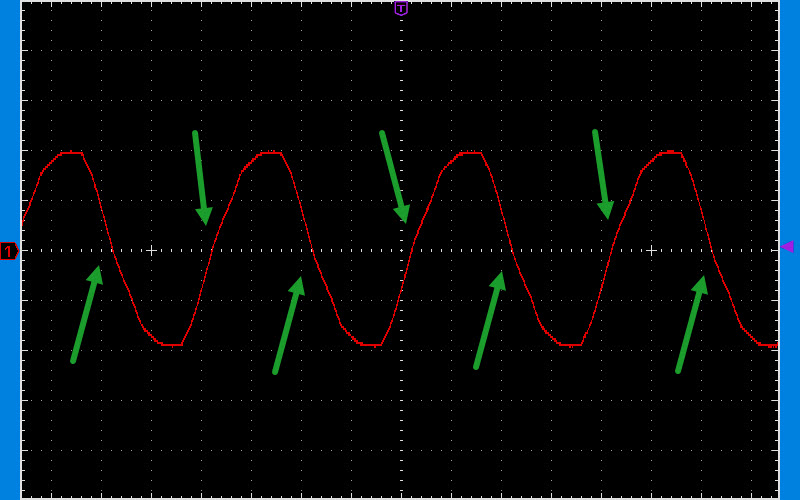
| Figure 1. | Mains sine wave (Green arrows show the zero crossing points). |
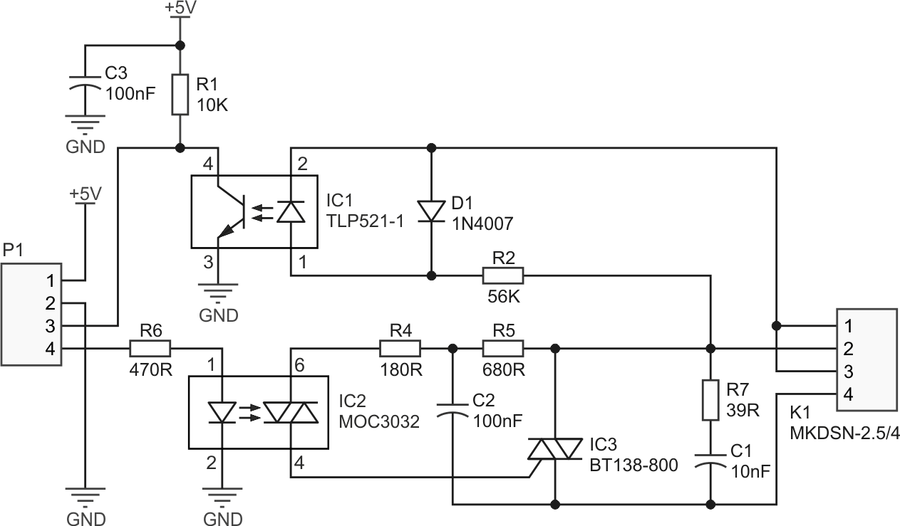
The Figure 1 shows the mains sinusoidal wave with the frequency of 50 Hz (sometimes 60 Hz). To build a dimmer, the zero crossing points (the points where the wave changes its polarity) are important. To grab these points, we have to use a zero crossing detector. The Figure 2 demonstrates the schematic diagram of the whole circuit.
 |
|
| Figure 2. | Schematic diagram of the digital AC dimmer. |
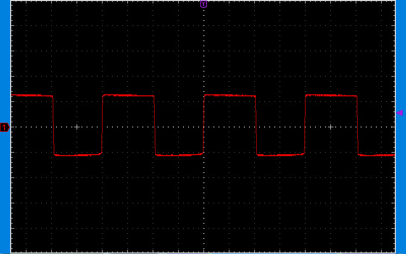
R1, R2, IC1, D1, and C3 build the zero crossing detector circuit. It is designed to make proper isolation (optically) with the mains voltage. So we can expect to get a noise-free signal which can be safely connected to the Arduino I/Os. The Figure 3 demonstrates the zero-crossing detector output signal (Pin-4 of the IC1). For sure you can use similar optocouplers as well, but I use this part for other designs as well and it does the job quite well.
 |
|
| Figure 3. | The output signal of the zero crossing detector circuit. |
So as it is clear, we gonna use the zero crossing pulse as a trigger for the main controlling circuit. Exactly after a trigger (a zero cross), in a simple term, we have to decide how much power we want to deliver. It is easier to understand by demonstrating the Arduino code and output wave later.
IC3 is a BT138 triac. The load is in series with the triac and the AC line, so the triac determine the amount of power that should be delivered to the load.
Attention: the mounting base of the BT138 triac (by default it is used to attach a heatsink) is connected to the Pin-2. It means you should never touch the heatsink or screw it to a metal enclosure!
R4, R5, and C2 implement a snubber circuit [1] for the IC2 and C1 and R7 make a snubber circuit [1] for IC3. These parts help the device to be compatible with a variety of loads, such as inductive loads.
IC2 is an opto-triac component which makes proper galvanic isolation between the digital side and the AC line. The selected part number is MOC3021. You can use similar part numbers also, but be careful not to use the parts with embedded zero crossing detector. Those parts are useful for switching the AC loads (ON/OFF), not for dimming.
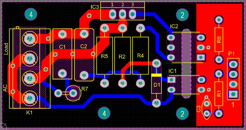
The Figure 4 shows the designed PCB layout. The AC lines which are supposed to carry a high amount of current have drawn thicker and double sided. In addition, both track sides have reinforced by some vias to reduce the resistance and increase the current transmission capability of the PCB track.
 |
|
| Figure 4. | The PCB layout of the AC dimmer. |
All components are DIP. Therefore it is easy for everyone to solder the components quickly and use the circuit as a module. R2, R4, R5, and R7 are 1 W resistors. R1 and R6 are ¼W. C1 and C2 can be selected from MKT or polyester type capacitors, but make sure that they are at least 400 V rated. The 250 V rated capacitors seem to be okay, but 250 V is a bit close to the input voltage boundaries. Therefore 400 V is a wise selection for the capacitors’ voltages. C1 has a 10 mm pitch size. This number is 10.5 mm for the C2. K1 is an MKDSN connector with 5.08 mm pitch size (MKDSN-2.5/4-5.08). P1 is a traditional 4 pins male header connector.
The PCB board has a cutout under the IC1 and IC2. It provides better galvanic isolation between two sections of the circuit board.
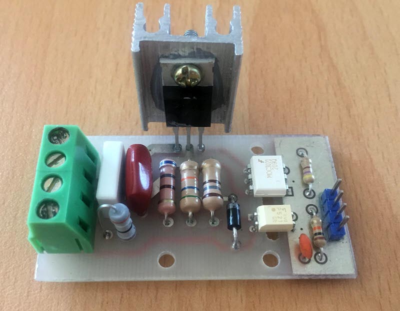
The Figure 5 demonstrates the first prototype of the circuit board. Gerber project files can be downloaded from the link at the end of the article.
 |
|
| Figure 5. | The first prototype of the circuit. |
The mounted heatsink is just for a short test. For an actual long term use, you must use a bigger heatsink. The location of IC3 (near the PCB border) makes the heatsink installation task much easier.
Now it’s the time to connect the circuit to an Arduino board and control the AC load. I selected an Arduino Nano which introduces enough resources for this project, but you can use other boards as well. A sample Arduino code for the AC dimmer is as follows:
1. const byte ZCP = 2;
2. const unsigned int dim = 5000;
3. void setup() {
4. pinMode(ZCP, INPUT);
5. pinMode(10, OUTPUT);
6. digitalWrite(10, LOW);
7. }
8. void loop() {
9. if (digitalRead(ZCP) == HIGH)
10. Zero_Cross();
11. }
12. void Zero_Cross() {
13. digitalWrite(10, LOW);
14. delayMicroseconds(dim);
15. digitalWrite(10, HIGH);
16. }
It is not necessary to write complex code to test our dimmer. There are two methods to sniff the zero crossing detector pulses: polling and interrupt. In the first attempt, I fixed this using an interrupt, but I faced the load flickering in some situations. The flickering is an annoying situation which happens with some dimmers. The reason is the wrong timing. As I mentioned earlier, the zero crossing points are quite important and any random time-shift will cause instability. Using an interrupt was introducing some jitter, and this jitter caused flickering in some dimmer settings. Therefore I switched the method to polling (lines 8 to 11).
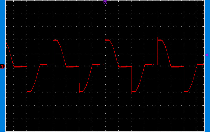
All we have to do is to change the triac off-time in both cycles, so the “dim” variable defines the transferred power to the load. As a starting point, I set the dimmer to the middle. That means for a duration of 5 ms, the triac is kept OFF. So let’s confirm our theory in practice by examining the load waveform.
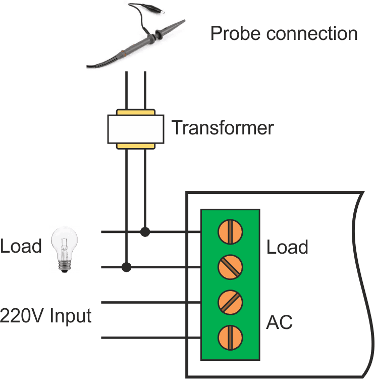
Be careful: never connect your oscilloscope probe directly to the mains. The probe’s ground connection can build a closed loop with the mains terminal and blow up everything in the path, including your circuit, probe or oscilloscope or even yourself!
There are several solutions to overcome this, such as using an isolator or using a differential probe … etc. I used an ordinary transformer (220 V to 12 V) and verified the output just by using this. Please check the Figure 6 for the connections. I have to note that the load must be connected, otherwise you won’t see the true waveform.
 |
|
| Figure 6. | Probing the load and required connections. |
The Figure 7 shows the output waveform (50%). You can expand the code and add two buttons to increase and decrease the output power. You can develop the code and modify it with your own Arduino board and your specific needs.
 |
|
| Figure 7. | The output waveform in 50% of the power (dim = 5000). |
