Integration of analog circuitry with digital logic often requires the addition of an extra supply rail or two. The excellent PSRR of precision op-amps (typically >>100 dB) makes them unfussy about power rail variations. This simplifies power supply circuitry and eases the task of designing it to be uncomplicated and inexpensive.
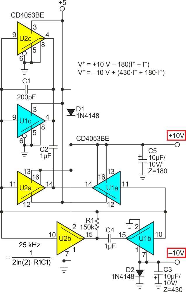
Here’s a variation on the popular flying-capacitor charge-pump voltage converter motif that takes advantage of op-amp tolerance for less than perfect supply regulation. It first doubles and then inverts 5 V to generate nominally symmetrical positive and negative 10-volt rails which can each handily supply several milliamps. The complete converter consists of two inexpensive generic 20 volt-capable, metal-gate CMOS triple SPDT CD4053Bs, plus just eight passive components. Figure 1 shows the circuit.
 |
|
| Figure 1. | A 25 kHz multivibrator (U2b) clocks flying capacitor switches that first, double 5 V to +10 V (paralleled U1a,c and U2a,c), and then inverts it to –10 V (U1b and U2b). |
Paralleled switches U1c and U2c, running at FPUMP = 25 kHz, alternate the top end of “flying” capacitor C2 between ground and +5 V, while U1a and U2a synchronously alternate its bottom end between +5 V and +10 V, creating a voltage-doubling capacitive charge pump. The connection of the resulting 10-V rail on U1,2 pin 13 to U1,2 pin 16 implements the first “bootstrap” mentioned above, whereby the switches supply 10 V to themselves. D1 gets things rolling on power up by initially providing ~+5 V until the charge pump takes over, whereupon D1 is reverse biased and disconnects.
Doubling up on the U1,2a and U1,2c charge pump switches serves to halve the effective impedance of the +10 V output to ~180 Ω. This is important because the +10 V output powers not only the external load, but also the internal U1,2b voltage inverter (more on this later). Plus, these relatively high ON-resistance metal-gate CMOS switches need all the help they can get. The result is a fairly stiff +10 V output that droops with loading current 180 mV/mA according to this expression:
V+ = 10 V – 180(I+ + I–).
Where:
I+ = +10 V output load current
I– = –10 V output load current
The 25 kHz pump clock is provided by a “merged” oscillator consisting of U2b driven by positive feedback. From U2c through C1 and negative feedback through R1, generating:

Pump frequency will vary somewhat with component tolerance and loading of the 10 V outputs, but since the clock frequency isn’t critical, any effect on pump performance will be insignificant.
The resulting oscillator waveforms are sketched in Figure 2.
 |
|
| Figure 2. | The 25 kHz multivibrator 10 V p-p waveshapes. |
Inversion of +10 V to produce –10 V is handled by U1,2b switching C4 between +10 V and ground on the left side and ground and –10 V on the right. The connection to pin 7 provides the second “bootstrap”. D2 clamps pin 7 near enough to ground for the switches to begin working at power-up until the charge pump takes over.
The result is a negative rail that reacts to loading according to this expression:
V– = –10 V + (430·I– + 180·I+).
Where:
I+ = +10 V output load current
I– = –10 V output load current
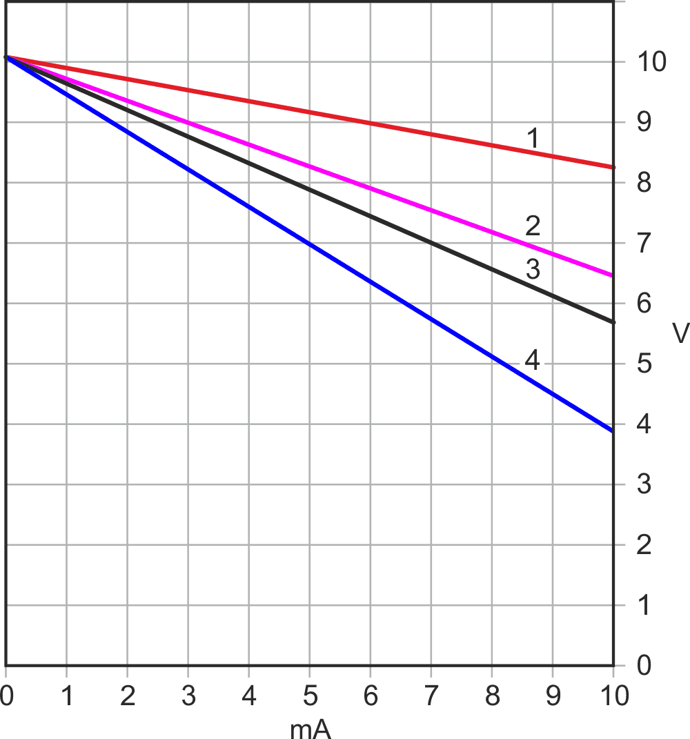
The dependence of the two output voltages on loading is graphically summarized in Figure 3.

